In recent years, the increase in the number of networks, stricter design constraints and wiring density, and the gradual migration to high-speed, high-density projects have exacerbated the complexity of the PCB. Fortunately, PCB design tools have been steadily developed in recent years to meet the challenges posed by this increasingly complex design field. A major change, the adoption of 3D capabilities, is expected to enable designers to take into account both design innovation and the competitiveness of the global market.
3D design challenges

Traditionally, board designers have relied on design prototypes to ensure the design's shape, fit, and functionality before manufacturing. Although feasible, this method has many shortcomings.
First, the designer cannot determine whether the board is suitable before manufacturing the actual prototype.
Second, this method generally leads to multiple prototypes during the design process.
Again, multiple prototypes are very time consuming and the average cost for a moderately complex design prototype is $8,929.
Any extra time or cost increase in the design process will not only affect the competitiveness of a company, but also hinder our advancement into new business. It is not difficult to understand why this method is not welcome.
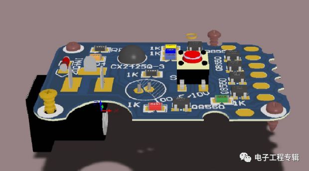
Another drawback is that PCB design is traditionally a two-dimensional design. Basically, the design is created in 2D, hand-labeled and passed to the mechanical design engineer.
Mechanical engineers use mechanical CAD software to redraw the design in 3D. Due to the complete manual operation, this method is very time-consuming and error-prone.
Therefore, it cannot provide competitive differentiation for the design of next-generation electronic products. Now that the problem is clear, board designers need to find better ways to view and analyze their increasingly complex designs.
The ultimate goal of PCB designers is to create products for the real world (with 3 dimensions), so the best solution is to use a design tool with advanced 3D capabilities.
It allows designers to view realistic 3D images before production, eliminating the need for prototypes and saving time and money. Accurate 3D models can be easily generated and then used for board layout in real 3D.
In addition, the 3D model of the target housing can be imported into the PCB design to ensure that the designed circuit board can be placed perfectly in this housing. Finally, designers can submit their design documents for production with confidence.
The 3D export function provides designers with the ability to perform further analysis in other analysis tools, such as thermal analysis and electromagnetic simulation analysis. For every type of compact battery-operated device that uses wireless connectivity today, the cooling effect is entirely dependent on the shape of the circuit board. This function is critical.
Because of these features, the 3D capabilities in PCB design tools are absolutely essential for the rapid, accurate and low-cost design of next-generation electronic products.
Full 3D function
The value of adding 3D capabilities to PCB design is undeniable, so many companies are now able to provide this functionality as a promotional point. However, the 3D capabilities provided by these design tools are quite different.
In order to take full advantage of 3D, it's not enough to just view real 3D images, but to extend to full 3D capabilities, including:
Ability to create 3D animation/video for design
With this feature, designers can easily share and showcase his product designs and even use them as marketing materials.
It can also promote better cooperation with other design teams or manufacturers. For example, with a 3D video, the designer can show the manufacturer the appearance of the assembled product. The video can also be used to illustrate the assembly sequence of the components on the circuit board.
Ability to import 3D models (including components) into board designs
Please note that some design tools lack this feature and only allow the designer to perform basic visualization and component gap checks in 2D.
However, if you can import the shell and other mechanical objects, you can ensure that the components are placed in the right place at the first time.
Ability to support 3D inspection in design rules
Since rules are real-time guides in the design process, this is a very important feature.
The 3D design rule checker tells the designer whether there is interference in the 3D space (on all axes) between the two components, between the components and the housing, or between the components and the heat sink.
Ability to model the copper layer in the PCB inner structure
Despite the use of ECAD packages with 3D capabilities, problems may still arise during the manufacturing process.
Finding problems at this stage of the design late in the design period will greatly increase costs. The ability to model the copper layer in the PCB's inner structure allows designers to easily view and verify the connection of pins to the inner layer or thermal reliefs.
The benefits of 3D design
Designing in 3D can bring you many benefits. It can reduce MCAD and ECAD iterative cycles to one cycle (in some cases, zero), thereby shortening the design cycle, and minimizing design errors, thereby greatly increasing production efficiency.
Moreover, by eliminating the uncertainty in the layout of the circuit board and the housing, designers can feel confident that they can focus on the aesthetic design of the product.
Other benefits of 3D design are:
Competitive Advantage
By improving communication within an organization and between suppliers and customers, 3D design speeds product design, makes manufacturing processes more efficient, and accelerates product promotion.
Lower design costs and improved profit margins, while the advancement of time to market and the improvement of product quality mean an increase in revenue.
Improve global cooperation
A realistic 3D design image can increase the efficiency of communication with suppliers, customers, and manufacturers. It even allows non-CAD personnel to participate in this process (for example, for customer surveys, explicit instructions, or product configurations).
This is particularly important in the current situation where many companies are inclined to external production (in China or local). Regardless of design intent or the desired end product, global design and manufacturing can easily introduce mistakes and misunderstandings.
The 3D design images provide a common, easy-to-understand platform that all team members can operate on.
More efficient design review and modification
The ability to create 3D renderings and animations simplifies the task of writing design plans and reviewing designs in design team members.
It also allows designers to easily implement changes and update the latest design changes. For example, once changes or modifications are made, a new 3D rendering or animation can be easily generated.
More efficient manufacturing and assembly processes
The 3D model provides a common basis for manufacturers to use it to work while also communicating design intent and related design details more accurately and clearly.
Errors previously discovered only after production can be discovered early in the design process. Therefore, using 3D models to manufacture and assemble products will be accurate and more efficient.
Promote sales and promote marketing
The product's 3D model can be a valuable marketing tool that allows customers to see the full picture of the product before it is produced, so the sales department can quickly make market assessment reports and help us bring additional benefits.
Conclusion
Over the years, real-time 3D graphics technology has completely changed the way that society interacts with computers. With 3D PCB design tools, this revolution has come to the PCB design field. It is changing the design and manufacturing methods of electronic products.
However, like any new technology or method, it is very important to find the best way to implement and use it. For PCB designers who want to benefit from 3D, this means choosing a software solution that offers full 3D capabilities.
This approach provides the functionality that circuit board designers need to help them create competitive next-generation electronic products in an increasingly complex design environment.
ZGAR bar 4000 Puffs
ZGAR electronic cigarette uses high-tech R&D, food grade disposable pod device and high-quality raw material. All package designs are Original IP. Our designer team is from Hong Kong. We have very high requirements for product quality, flavors taste and packaging design. The E-liquid is imported, materials are food grade, and assembly plant is medical-grade dust-free workshops.
Our products include disposable e-cigarettes, rechargeable e-cigarettes, rechargreable disposable vape pen, and various of flavors of cigarette cartridges. From 600puffs to 5000puffs, ZGAR bar Disposable offer high-tech R&D, E-cigarette improves battery capacity, We offer various of flavors and support customization. And printing designs can be customized. We have our own professional team and competitive quotations for any OEM or ODM works.
We supply OEM rechargeable disposable vape pen,OEM disposable electronic cigarette,ODM disposable vape pen,ODM disposable electronic cigarette,OEM/ODM vape pen e-cigarette,OEM/ODM atomizer device.

ZGAR bar 4000 Puffs Disposable Vape, bar 4000puffs,ZGAR bar 4000 Puffs disposable,ZGAR bar 4000 Puffs,ZGAR bar 4000 Puffs OEM/ODM disposable vape pen atomizer Device E-cig
ZGAR INTERNATIONAL(HK)CO., LIMITED , https://www.zgarvapepen.com