1 Introduction
The LED (light emitting diode) display is composed of an array of light emitting diodes. Light-emitting diode (LED) is a current control device with high brightness, small volume, good monochromaticity, fast response, simple driving, long life, etc. It can be used for real-time, diversity and dynamic in various occasions. The information release task has been widely used. The LED large screen is a display screen composed of an array of LED devices through a certain control mode for displaying various information such as text, images, and quotes, as well as television and video signals. As an important media for modern information release, LED large screen is receiving great attention from all walks of life, especially the business and advertising circles. It is widely used in industry, transportation, commerce, advertising, finance, sports competitions, simulated military exercises, and electronic landscapes. And other fields.
This paper introduces an 8-bit parallel input LED display driver chip, which realizes multi-color 256-level gray scale display from white to black in the large-screen LED display system. The picture is stable and clear, and has achieved good visual effects.
2 large screen LED system composition
Considering the electrical characteristics of LEDs and the requirements of practical applications such as mechanical installation, whether it is an indoor LED electronic display system or an outdoor LED electronic display, the structure is in the form of standard unit blocks, that is, 16×16, 16×32. 24 x 24 or 32 x 32 display pixel tubes constitute one unit block. Each unit block forms its own independent electronic scanning function, control function, storage function, and constitutes an independent subsystem; then, after each standard source and communication driving component, it forms a full dot matrix LED large screen electronic The display system, together with certain computer control components, multimedia card with digital component output or DVI card and power memory communication drive components, constitutes a full dot matrix LED large-screen electronic display system. The structural block diagram of the system is shown in Figure 1.
The core part is the LED scanning control chip, which is also the focus of this article. The chip is an 8-bit parallel input LED display drive structure, which can drive a 16×8 LED screen body. The application can be used to display a large LED screen through multiple cascades on the LED large screen.
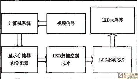
Figure 1 LED large screen system block diagram
Research on 3LED scanning method and control chip
1. Research on grayscale scanning method
For high-gray LED large-screen display, the grayscale layering (grayscale scanning) method is the key to the video controller design. Since the LED luminance is approximately proportional to the illumination time in the scanning period, the grayscale is grayscale. The implementation of the level is usually achieved by controlling the ratio of the LED's illumination time to the scan period, ie, using the modulation duty cycle.
(1) Grayscale scanning constraint formula
It is assumed that the number of display gray levels is N, and since the corresponding lighting time of the pixels with the gray level of 1 is td, the data display time of the gray level i after the gray linear modulation is itd, and the gray level is the highest. The data display time is (N-1)×td. The usual consideration is to complete a read of one line of data in the memory in td, and at the same time, the read line of data is hit to the screen for gray scale display in the period of td. . Since there are a total of N gray levels, the frame scan period is:
T=n×td×m(1)
Screen display efficiency: η = (N - l) × td × m / T = (N - l) / N (2)
Let the video data input rate be VI, and the memory read rate be Vo. Since one line of data in the memory unit must be read in td, there is: Vo/Vi>=h/(td×n)(3)
Let λ be the ratio of the memory readout and the input rate, that is, λ=Vo/Vi, and the formula (1) in the formula (3): λ>=h×N×m/(T×n) 4)
In order to ensure stable display of the image, the scanning frame rate must be high enough, set F>=F0 (ie T<=T0, T0=1/F0), F0 is the scanning frame rate acceptable by the human eye (F0>=60), substituted (4) Formula:
λ>=h×N×m/(T0×n)(5)
Substituting (1) gives: td=T0/(N×m)(6)
Equations (5) and (6) are grayscale scanning constraint formulas.
(2) 256 gray level full screen scanning
For 256 grayscale full screen scans, high gray levels, high scan frame rates, and low memory read rates are contradictory. In order to obtain a high number of gray levels, it is necessary to increase the memory read rate or reduce the frame scan frequency. When the number of gray levels is high, it is difficult to achieve the balance of the current integrated circuit. One of the solutions is to use a large number of parallel structures, but the cost per doubling of the scanning frequency is nearly doubled, and the complexity of the circuit is also increased. Another method is to properly sacrifice the display efficiency of the screen to obtain a frame. A compromise between frequency and rate, this method has been proven to be feasible.
In the design, considering the compromise between the frame rate and the display efficiency of the LED screen, λ=l, td=h/16, that is, the memory readout rate is equal to the data input rate, and the display basic time unit is 1/16 times the line period. The grayscale scanning is realized by the method of bitwise time-division display of the grayscale data, that is, when the computer screen image is output at 24 bits per pixel (8 bits each of red, green, and blue), by assigning different bits to different bits of each color sbit byte. The display time reaches the purpose of grayscale display. For example, the lowest bit (8th bit) corresponds to 1/16 line display time, the 7th bit corresponds to 1/8 line display time, ?, the 2nd bit corresponds to 4 lines of display time, and the highest bit corresponds to 8 lines of display time. The screen data update time is in units of line periods, and the lowest bit corresponds to the update time of 1 line time, in which 1/l6 line time is displayed, and in the remaining 15/16 lines, the blanking signal is generated by the control circuit for blanking, and the remaining bits are Similar.
2, LED scanning control chip
After comparing the data, this paper adopts the constant current source driving method, and designs a control unit that can realize 256-level gray scale display from white to black. The display control chip has an 8-bit parallel input port synchronized with the clock, and contains 16 8-bit shift registers and 16 8-bit data latches, which can shift and latch 8-bit parallel data. 2 is a circuit diagram of the scanning and display control chip.
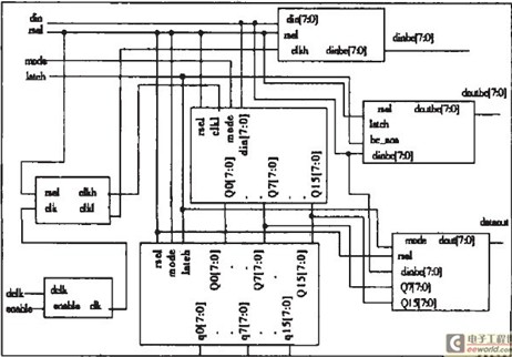
Figure 2. Scan and display control chip circuit diagram
When the circuit starts to work, the 8-bit parallel data is driven into the shift register module of the chip under the action of the shift clock pulse. The internal contains 16 shift registers, so after 16 shifts, the data will be from the chip. DOUT0~DOUT7 are output to the next chip; at the same time, 16 8-bit data obtained by shifting are input into the latch to be latched. At this time, as long as the output control signal is low, and the row strobe signal of the same-named row is given at the same time to make the output open, each column can start to output a constant current, and the 8-bit counter starts counting the gray-scale clock, when the count value is When the gray values ​​stored in the column are equal, the constant current output of the column ends, thereby realizing the display time control of the corresponding LED, that is, the duty ratio control. If 10 display control units are used to drive the LED display in cascade, the first line of data can be transmitted by shifting 160 times in parallel.
The code is written in VerilogHDL and compiled and simulated by Modelsim simulation software. The timing diagram shown in Figure 3 and Figure 4 is obtained.
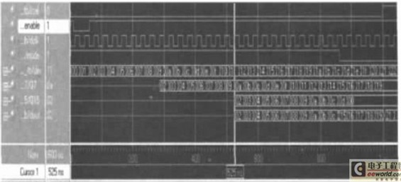
Figure 3 gray control unit timing diagram
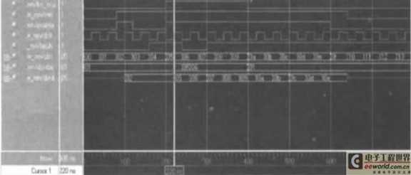
Figure 4 brightness control unit timing diagram
Through the timing diagram we can see on the control side:
Under the control of the control terminals such as enable, rsel, bc_ena, and latch, different gray levels and brightness can be realized according to different requirements. In the gray control unit, the data is shifted and transmitted to the output after 16 pulses, and the 8-column or 16-column output is adjustable; in the brightness control unit, by adjusting the enable, bc_ena, latch The value realizes the adjustment of the output data, thereby accurately implementing the brightness control function.
According to the display time of the same-named line of each part is equal to the display time of the same-named line, the value of the line period and the point (column) period can be obtained, that is, the line period = the number of lines of the frame period/scan mode, the dot period = the line period / (per Line points × part number). If the frame rate is 120 Hz, the frame period is 1/120 s = 8.33 ms. According to the scanning mode of 1/16, 80 lines can be divided into 5 16 rows, 160 columns per row, so that the line period is 520.6 μs; The period is 650.75 ns; the point frequency is 1.54×10⁶ Hz.
4 Conclusion
This paper discusses the grayscale scanning method in LED large-screen video controller. This paper proposes the implementation scheme of 256 grayscale scanning. The author's innovation lies in designing a 256-level grayscale display from dark to bright. LED display control chip, in this design, the frame rate can reach 120Hz, the line period is 520.6μs, the dot period is 650.75ns, and the point frequency is 1.54×10⁶Hz. The chip can drive LED large screen through multiple cascades. Good application prospects.
Low Voltage Electrical Switchgear
Low Voltage Electrical Switchgear,Indoor Low Voltage Electrical Switchgear,Low Voltage Electric Switchgear
Shenzhen Hongyan Wire Industry Co., Ltd. , https://www.hy-cable.com