The SIA’s report showed that the global semiconductor capacity utilization rate was 92.2% in the second quarter of 2011, but due to participation in the fundamental changes, it was unable to announce the growth rate compared with the previous quarter. According to SIA, the statistical report's participation in the most fundamental changes is that Taiwanese companies TSMC, UMC and Nanya Technology are no longer participating in SICAS; in addition, National Semiconductor (NS) has also become a Texas company. Instruments (TI) disappeared and disappeared on the statistical list.
“Taiwan has no longer participated in the plan and two other Taiwanese manufacturers have followed suit,†said Ebun Caldeira, director of finance and market research for SIA, who declined to explain why TSMC exited. “We are trying to persuade TSMC to rejoin,†she said. If TSMC agrees to return in a short time, it may re-release the second quarter data.
The time for the SIA to release the second quarter of the semiconductor production statistics report is also considered to be a bit later than in previous years; the report shows that the overall semiconductor manufacturing capacity in the quarter was 1.93 million wafers per week (waspstartsperweek, WspW). This data was 2.25 million WspW in the first quarter.
Bill McClean, president of market research firm ICInsights, pointed out that the current SICAS statistics can only represent about 57% of the actual semiconductor fab manufacturing capacity; this ratio was 88% at the beginning of the 1990s report. Before the exit of TSMC, UMC, and South Asia Branch, SICAS's statistical report represents more than 70% of global wafer manufacturing capacity.
"The report's representation of global semiconductor production capacity is getting lower and lower, which is really regrettable, because the statistics were originally a very useful tool." McClean said that the statistics are useful for estimating the level of semiconductor capacity utilization because participation The plan's manufacturers still have a considerable contribution to overall semiconductor capacity utilization.
But why does TSMC exit the statistics? McClean speculated that it may be because TSMC and UMC’s two foundry giants no longer wish to have too detailed production capacity data exposed each month. He pointed out that the WSTS also stopped publishing programmable logic component capacity data a few years ago, mainly because of the rise of two major suppliers, Xilinx and Altera, who did not want to disclose detailed monthly sales figures. .
According to the SICAS report, global semiconductor capacity utilization rate was 92.2% in the second quarter, which was 93.7% in the first quarter. One of the more mature processes of 0.12 micron and 8-inch wafer processes has a capacity utilization rate of 80 to 90%; the more advanced processes under 0.12 micron and the 12-inch wafer process capacity utilization rate are over 90%.
In addition, the report also shows that the semiconductor manufacturing capacity of the process node below 50 nm is 98.85 WspW in the second quarter, accounting for about 50% of the global semiconductor production capacity, and the capacity utilization rate is 96.7%; the same time the 12-inch wafer The capacity is 1.11 million WspW and the capacity utilization rate is 95.6%.
The SICAS organization was jointly established and sponsored by the leading semiconductor industry associations around the world in 1994, but the statistical activity was implemented and managed by a committee composed of representatives of industry associations from various regions; currently it seems that the Taiwan Semiconductor Industry Association (TSIA) ) is not one of them.
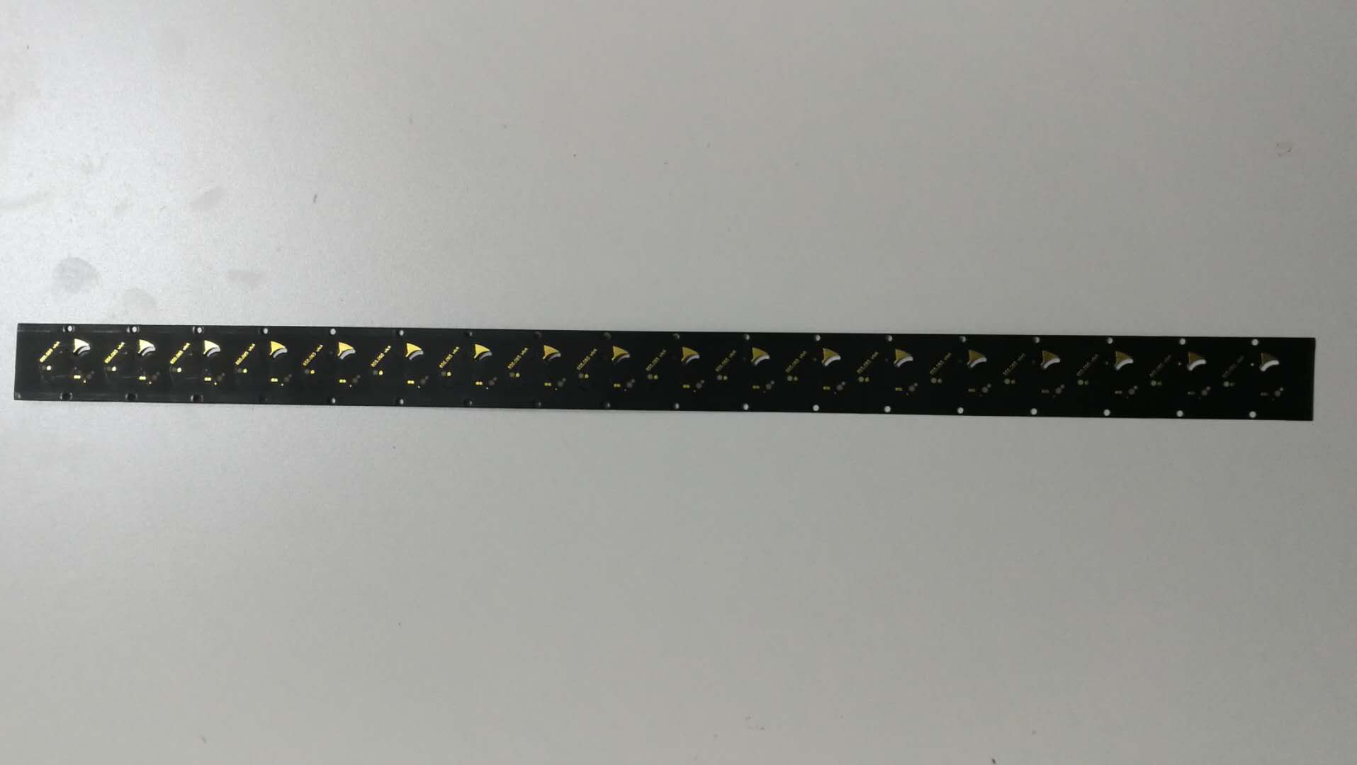
Double Side Board, Base Material: FR4 TG135. copper thickneess 1oz finished. Immersion Gold surface treatment with matt black soldermask. Thin board thickness 0.2mm. Min.line width/Min.line spacing 0.15/0.15mm. E-test: 100%
The double-side-board is one of the most products we produce. Our double-sided plate thickness can be treated from the 0.2-5.0mm. and we can do the surface treatment can be ENIG, HASL, LF-HASL, Immersion Tin,Immersion silver,Flash Gold(Gold plating), OSP and etc.

Double Side Board
Double Side Board,Double Sided PCB,Double Sided PCB Board,PCB Circuit Board
Orilind Limited Company , http://www.orilind.com