The DS1337 serial real-time clock chip is a low-power, all-BCD-coded clock calendar chip with two programmable timed alarms and a programmable square wave output. Its address and data can be transmitted serially over the I2C bus, providing information such as seconds, minutes, hours, days, weeks, months, and years.
1.1 Pin Description of DS1337
The pin arrangement diagram of the DS1337 is shown in Figure 1. The function of each pin is as follows:
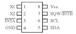
Figure 1 DS1337 pin diagram
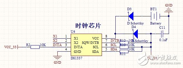
VCC, GND: DC power supply and ground. The input range of VCC is between 1.8~5.5V. X1, X2: The standard 32.768kHz quartz crystal access terminal, the internal crystal oscillator circuit design requires a specific capacitive load of 6pF. In addition, these two pins can also have other connections, that is, the X1 pin is connected to the external oscillating signal source, and the X2 pin is left floating.
SCL: Serial clock input used to synchronize data transfers on the bus.
SDA: Serial data input and output, SDA is the data input and output pin of I2C bus interface, open-drain output, requires a pull-up resistor when used.
SQW/INTB: Square wave/interrupt output. The internal control register of the DS1337 can be programmed to control whether this pin is an output square wave or an output interrupt signal. This pin is an open-drain output and is connected to an external pull-up resistor.
INTA: Interrupt output. When enabled, if the set value of the alarm register matches the current time, the pin will output a low level. This pin is also an open-drain output, which is connected to a pull-up resistor.
1.2 time register
The commonly used time register address is 00H~06H. The setup and initialization time and calendar can be achieved by writing the corresponding register field, which is represented by the BCD code. The DS1337 can work in either 12-hour mode or 24-hour mode. Bit 6 of the hour register is defined as a 12-hour mode or a 24-hour mode selection bit. When this bit is 1, the 12-hour mode is selected. In the 12-hour mode, bit 5 is the AM/PM flag, and when this bit is 1, it indicates PM. When in the 24-hour mode, bit 5 is the second ten (representing 20 to 23 hours). The seventh bit of the month register is the century bit, which changes when the register overflows from 0 to 99.
1.3 Control Registers and Status Registers
The DS1337 has a control register and a status register that can be used to control the output of the real-time clock, alarm, and square wave.
The control register address is 0EH. among them:
EOSC: Oscillator enable bit. This bit is 0, the oscillator starts to vibrate; when 1, the oscillator stops. When power is first applied, this bit is 0; RS1, RS2: Square wave output frequency selection bit. There are four combinations of RS1 and RS2, and the corresponding square wave output frequencies are 1 Hz, 4.096 kHz, 8.192 kHz, and 32.768 kHz. At the time of power up, the square wave output frequency setting is 32.768 kHz.
INTCN: Interrupt control bit. Used to control the relationship between two alarms and the interrupt output pin. When 1, the two alarms have independent interrupt outputs when they meet the timing conditions. When 0, the two alarms share an interrupt output pin INTA, and the foot SQW/INTB is a square wave output. This bit is 0 when power is first applied.
A1IE: Alarm 1 interrupt enable bit. When 1, the A1F bit of the status register is allowed to be output to pin INTA. This bit is 0 on power-up. At this time, the IN1 signal cannot be initialized with the A1F bit.
A2IE: Alarm 2 interrupt enable bit, this bit has the same effect as the A1IE bit.
The status register address of the DS1337 is 0FH. The functions of each bit are as follows:
OSF: Oscillator stop flag. This bit is 1, indicating that the oscillator has stopped. There are four cases that can produce such a result: first, the chip is just powered on, second, the Vcc pin voltage is insufficient, third is the EOSC bit is 1, and fourth, the crystal oscillator is externally affected (such as noise).
A1F, A2F: Alarm clock flag. When 1, it means that the alarm set time matches the current time and an interrupt output is generated.
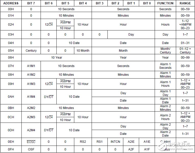
Figure 2 DS1337 register
1.4 Reading and writing to DS1337
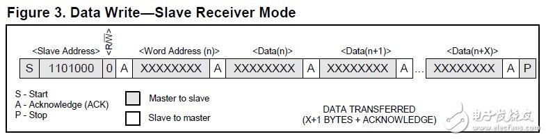
Figure 3 DS1337 write register
From the above figure, it can be seen that the master initiates the start condition, sends the address of the slave and the write command (0xD0|0x00), waits for the slave's response, and then sends the register address to be written, waiting for the slave's response. Then send the data to be written, wait for the response from the slave, and if the write is completed, the master sends the end. Complete the data write process once.
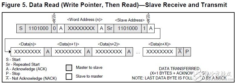
Figure 4 DS1337 read register
From the above figure, it can be seen that the master initiates the start condition, sends the address of the slave and the write command (0xD0|0x00), waits for the slave's response, and then sends the register address to be read, waiting for the slave's response. The master then resends the start condition, sends the slave's address and read command (0xD0|0x01), waits for the slave's response, receives the slave's data, and the master responds. When the last data is received, the master sends a non-acknowledgement and an end. Complete a read data process.
Second, the introduction of SMBus busThe SMBus serial I/O interface is a two-wire bidirectional serial bus that is compatible with the I2C serial bus. Figure 5 shows a typical SMBus configuration. The operating voltage of the SMBus interface can be between 3.0V and 5.0V, and the operating voltage of different devices on the bus can be different. The SCL (serial clock) and SDA (serial data) lines are bidirectional. They must be connected to the supply voltage by pull-up resistors or similar. Both lines are pulled high when the bus is idle. The SCL and SDA of each device connected to the bus must be open-drain or open-collector.
Figure 5 SMBus configuration
2.1 handshake
SMBus uses a variety of line conditions as a handshake signal between devices. In a data transfer, SDA can only change the level when SCL is low. The change in SDA when SCL is high is the start and stop signals that represent the following:
Start: This condition initiates a transfer process. A falling edge appears on SDA when SCL is high.
End: This condition ends a transfer process. A rising edge appears on SDA when SCL is high.
Acknowledgement: Also known as ACK, the receiving device sends this signal to indicate acknowledgment. For example, after device X receives a byte, it will send an ACK to confirm the transfer was successful. The ACK condition is to sample SDA low when SCL is high.
Non-acknowledgement: Also known as NACK, this is sampled to SDA high when SCL is high. When the receiving device cannot generate an ACK, the transmitting device sees a NACK. In a typical data transmission, a NACK signal is received indicating that the addressed slave is not ready or not on the bus. A master in the receiving state sends a NACK indicating that this is the last byte of the transmission. Figure 2 shows the handshake signal timing.

Figure 6 SMBus timing
2.2 Transmission method
There are two possible modes of transmission: write (from master to slave) and read (from slave to master). In a single transmission, any device can be one of four roles. These four roles will be explained below. Note that the slave address +R/W' refers to an 8-bit transfer (7-bit address, 1 bit R/W).
1) Master Transmitter: In this mode, the device transmits serial data on SDA and outputs a clock on SCL. The device initiates the transfer with a start condition, sends the slave address +W, and then waits for an ACK from the slave. After receiving the ACK, the device transmits one or more bytes of data, each of which is acknowledged by the slave. After the last byte has been transmitted, the device sends a Stop condition.
2) Master Receiver: In this mode, the device receives serial data on SDA and outputs a clock on SCL. The device initiates the transfer with a start condition and then transmits the slave address +R. After receiving the ACK of the slave pair address, the clock is output on SCL and received on SDA. After receiving the last byte, the device will send a NACK and a stop condition.
3) Slave Transmitter: In this mode, the device outputs serial data on SDA and accepts the clock on SCL. The device receives a start condition and its own slave address +R, then issues an ACK and enters the slave transmit mode. The device sends data on SDA and receives an ACK after each byte has been transmitted. After the last byte has been transmitted, the master sends a NACK and a Stop condition.
4) Slave Receiver: In this mode, the device receives the start condition from the master and its own slave address +W. Then issue an ACK and enter the slave receive mode. The device now receives serial data on SDA and receives the clock on SCL. An ACK is sent after each byte is received, and the slave receive mode is exited after receiving the stop condition of the master device.
Figure 7 shows a typical write operation. Figure 8 shows a typical read operation.
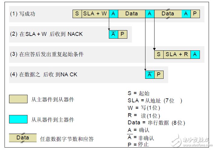
Figure 7 write operation
(1) is a successful transfer process. In (3), the master resends the start condition after receiving an ACK. This process allows the master to initiate a new transfer process (for example, switching from a write operation to a read operation) without abandoning the bus. Repeated start conditions are typically used when accessing the EEPROM because a read operation must have an operation to write to the memory address.
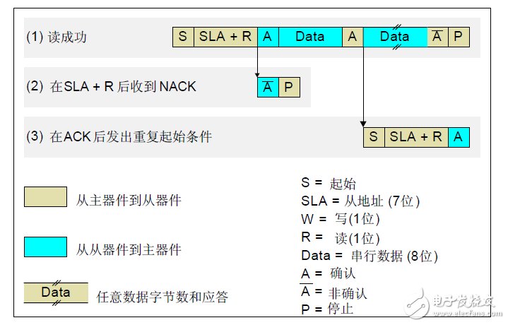
Figure 8 read operation
2.3 SMBus Special Function Register
Access and control of the SMBus serial interface is accomplished through five special function registers: control register SMB0CN, clock rate register SMB0CR, address register SMB0ADR, data register SMB0DAT, and status register SMB0STA. System devices can have one or more SMBus serial interfaces.
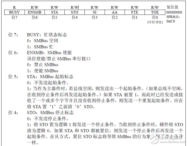
2.3.1 Control Register SMB0CN
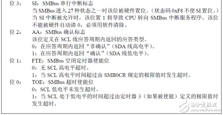
The SMBus Control Register SMB0CN is used to configure and control the SMBus interface. All bits in this register can be read and written in software. There are two control bits that are also affected by the SMBus hardware. When a valid serial interrupt condition occurs, the serial interrupt flag (SI, SMB0CN.3) is set to logic 1 by hardware and can only be cleared by software. The stop flag (STO, SMB0CN.4) is cleared by hardware when a stop condition occurs on the bus.
2.3.2 Clock Rate Register SMB0CR
The SMBus clock register is used to control the SCL clock rate while the device is operating in master mode. The 8-bit number in SMB0CR determines the clock rate, and the formula is as follows:

Among them, SMB0CR is a complement of a negative number. Therefore, for the SCL frequency of 100kHz and the SYSCLK of 16MHz, -80, ie 0xB0, should be loaded into SMB0CL.
2.3.3 Address Register SMB0ADR
The SMBus address register holds the slave address that the device will acknowledge in the slave mode. Bit (7:1) holds the slave address; bit 0 is the general call allowed. If Bit 0 is set, the device will acknowledge the general call address (0x00).
2.3.4 Data Register SMB0DAT
The SMBus data register is used to hold data to be sent or just received. The data read from this register is valid only when SI=1. When SI is not 1, SMBus may be in the process of moving data into or out of SMB0DAT. Note: During transmission, the highest bit shifted out of SMB0DAT is moved back to the lowest bit, so the original data is still stored in SMB0DAT after a transfer is completed.
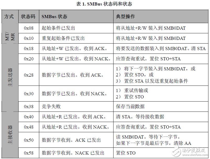
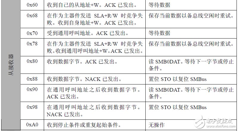
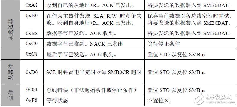
1.3.5 Status Register SMB0STA
There are 28 possible SMBus states, each corresponding to a unique status code. The upper 5 bits of the status code are variable, and a valid status code
The lower 3 bits are fixed to 0 (when SI=1). Therefore all valid status codes are integer multiples of 8.
3.1 Hardware
3.2 Software
1 typedef struct
2 {
3 u8 second; // 0 to 59
4 u8 minute; // 0 to 59
5 u8 hour; // 0 to 23 (24-hour TIme)
6 u8 day; // 0 = Sunday, 1 = Monday, etc.
7 u8 date; // 1 to 31
8 u8 month; // 1 to 12
9 u8 year; // 00 to 99
10 } DS1337_TIme;
11
12 xdata DS1337_TIme TIme;
13
14 bit SMB_BUSY;
15 u8 COMMAND;
16 u8 Mode;
17 u8 wr_data[2];
18 u8 wrnumber;
19 u8 get_data;
20
twenty one
22 void DS1337_Set_time(DS1337_time dt);
twenty three
twenty four
25 char bcd2bin(char bcd_value)
26 {
27 char temp;
28 temp = bcd_value;
29 temp 》》= 1;
30 temp &= 0x78;
31 return(temp + (temp 》》 2) + (bcd_value & 0x0f));
32 }
33
34
35 unsigned char bin2bcd(unsigned char value)
36 {
37 char retval;
38 retval = 0;
39
40 while(1)
41 {
42 if(value 》= 10)
43 {
44 value -= 10;
45 retval += 0x10;
46 }
47 else
48 {
49 retval += value;
50 break;
51 }
52 }
53 return(retval);
The function of line 25 is to convert the BCD code into a binary number. The function of line 35 is to convert the binary number to a BCD code.
1 void init_iic(void)
2 {
3 SMB0CN = 0x44; // Enable SMBus with acknowledge low (AA = 1)
4 SMB0CR = 146; // SMBus clock rate = 100 kHz 146
5 EIE1 “= 2; // SMBus interrupt enable
6 SI = 0;
7 SMB_BUSY = 1;
8 }
9
10
11 void Write_DS1337(u8 adrress, u8 data1)
12 {
13 Mode = 1;
14 wrnumber = 2 ;
15 wr_data[0] = adrress;
16 wr_data[1] = data1;
17 SMB0CN = 0x44;
18 COMMAND = DS1337_ADDR;
19 STO = 0;
20 STA = 1;
21 SMB_BUSY = 1;
22 while(SMB_BUSY);
twenty three }
twenty four
25
26 int Read_DS1337(u8 adrress)
27 {
28 Mode=0;
29 SMB0CN = 0x44;
30 COMMAND = (DS1337_ADDR | 0x01);
31 wr_data[0] = adrress;
32 STO = 0;
33 STA = 1;
34 SMB_BUSY = 1;
35 while(SMB_BUSY);
36 return get_data;
37 }
The function of line 1 initializes the SMBus bus. The function on line 11 is the DS1337 write operation. The function on line 26 is the DS1337 read operation.
1 void DS1337_init()
2 {
3 u8 status;
4 DS1337_time DT;
5
6 DT.second = 30;
7 DT.minute = 50;
8 DT.hour = 21;
9 DT.day = 2;
10 DT.date = 12;
11 DT.month = 8;
12 DT.year = 14;
13
14 status = Read_DS1337(DS1337_STATUS_REG);
15 if((status & 0x80) != 0)
16 {
17 DS1337_Set_time(DT);
18 Write_DS1337 (DS1337_CONTROL_REG, DS1337_CTRL_REG_INIT_VAL);
19 Write_DS1337 (DS1337_STATUS_REG, DS1337_CLEAR_STATUS_VAL);
20 }
twenty one }
twenty two
23 void DS1337_Set_time(DS1337_time dt)
twenty four {
25 u8 bcd_sec, bcd_min, bcd_hrs, bcd_day, bcd_date, bcd_mon, bcd_year;
26
27 bcd_sec = bin2bcd(dt.second);
28 bcd_min = bin2bcd(dt.minute);
29 bcd_hrs = bin2bcd(dt.hour);
30 bcd_day = bin2bcd(dt.day);
31 bcd_date = bin2bcd(dt.date);
32 bcd_mon = bin2bcd(dt.month);
33 bcd_year = bin2bcd(dt.year);
34
35 Write_DS1337 (DS1337_SECONDS_REG, bcd_sec);
36 Write_DS1337 (DS1337_MINUTES_REG, bcd_min);
37 Write_DS1337 (DS1337_HOURS_REG, bcd_hrs);
38 Write_DS1337 (DS1337_DAY_OF_WEEK_REG, bcd_day);
39 Write_DS1337 (DS1337_DATE_REG, bcd_date);
40 Write_DS1337 (DS1337_MONTH_REG, bcd_mon);
41 Write_DS1337 (DS1337_YEAR_REG, bcd_year);
42 }
43
44 void DS1337_Get_time()
45 {
46 u8 bcd_sec, bcd_min, bcd_hrs, bcd_day, bcd_date, bcd_mon, bcd_year;
47
48 bcd_sec = Read_DS1337(DS1337_SECONDS_REG);
49 bcd_min = Read_DS1337 (DS1337_MINUTES_REG);
50 bcd_hrs = Read_DS1337(DS1337_HOURS_REG);
51 bcd_day = Read_DS1337 (DS1337_DAY_OF_WEEK_REG);
52 bcd_date = Read_DS1337 (DS1337_DATE_REG);
53 bcd_mon = Read_DS1337(DS1337_MONTH_REG);
54 bcd_year = Read_DS1337(DS1337_YEAR_REG);
55
56 Time.second = bcd2bin(bcd_sec);
57 Time.minute = bcd2bin(bcd_min);
58 Time.hour = bcd2bin(bcd_hrs);
59 Time.day = bcd2bin(bcd_day);
60 Time.date = bcd2bin(bcd_date);
61 Time.month = bcd2bin(bcd_mon);
62 Time.year = bcd2bin(bcd_year);
63 }
The function of the first line is to initialize DS1337, read the status register, and if the highest bit is not 0, the initialization time. The function of line 23 is to set the time, including the year, month, day, week, minute, minute, and second. The function on line 44 is the read time.
1 #ifdef eclipse
2 void SMBUS_ISR(void)
3 #else
4 void SMBUS_ISR (void) interrupt ESMB0_VECTOR
5 #endif
6 {
7 switch (SMB0STA)
8 {
9 case SMB_START: //Start condition sent
10 SMB0DAT = (COMMAND & 0xFE);
11 STA = 0;
12 break;
13 case SMB_RP_START: //Repeat start condition sent
14 SMB0DAT = COMMAND;
15 STA = 0;
16 break;
17 case SMB_MTADDACK: //Address + WRITE has been sent, received ACK
18 SMB0DAT = wr_data[0];
19 break;
20 case SMB_MTADDNACK: //Address + WRITE has been sent and received a NACK.
21 STO = 1; //Send STOP + START to try again
22 STA = 1;
23 break;
24 case SMB_MTDBACK: //The data byte has been sent and an ACK has been received.
25 switch(Mode)
26 {
27 case 1:
28 wrnumber--;
29 if(wrnumber)
30 SMB0DAT = wr_data[1];
31 else
32 {
33 STO = 1;
34 SMB_BUSY=0;
35 }
36 break;
37 case 0:
38 STA = 1;
39 break;
40 default:
41 STO = 1;
42 SMB_BUSY = 0;
43 break;
44 }
45 break;
46 case SMB_MTDBNACK: //data byte
46 case SMB_MTDBNACK: //The data byte has been sent and a NACK has been received.
47 STO = 1;
48 STA = 1;
49 break;
50 case SMB_MTARBLOST: //Competition failed
51 STO = 1;
52 STA = 1;
53 break;
54 case SMB_MRADDACK: //Address + READ has been sent. Received ACK
55 AA = 0;
56 break;
57 case SMB_MRADDNACK: //Address + READ has been sent. Received NACK
58 STO = 0;
59 STA = 1;
60 break;
61 case SMB_MRDBACK: //Received data bytes. ACK has been sent
62 get_data = SMB0DAT;
63 SMB_BUSY = 0; //Complete
64 STO = 1;
65 break;
66 case SMB_MRDBNACK: //Received data byte. NACK has been sent
67 get_data = SMB0DAT;
68 SMB_BUSY = 0;
69 STO = 1;
70 break;
71 default:
72 STO = 1;
73 break;
74 }
75 SI = 0;
76 }
SMBus interrupt, you need to manually clear the interrupt flag.
3.3 Physical
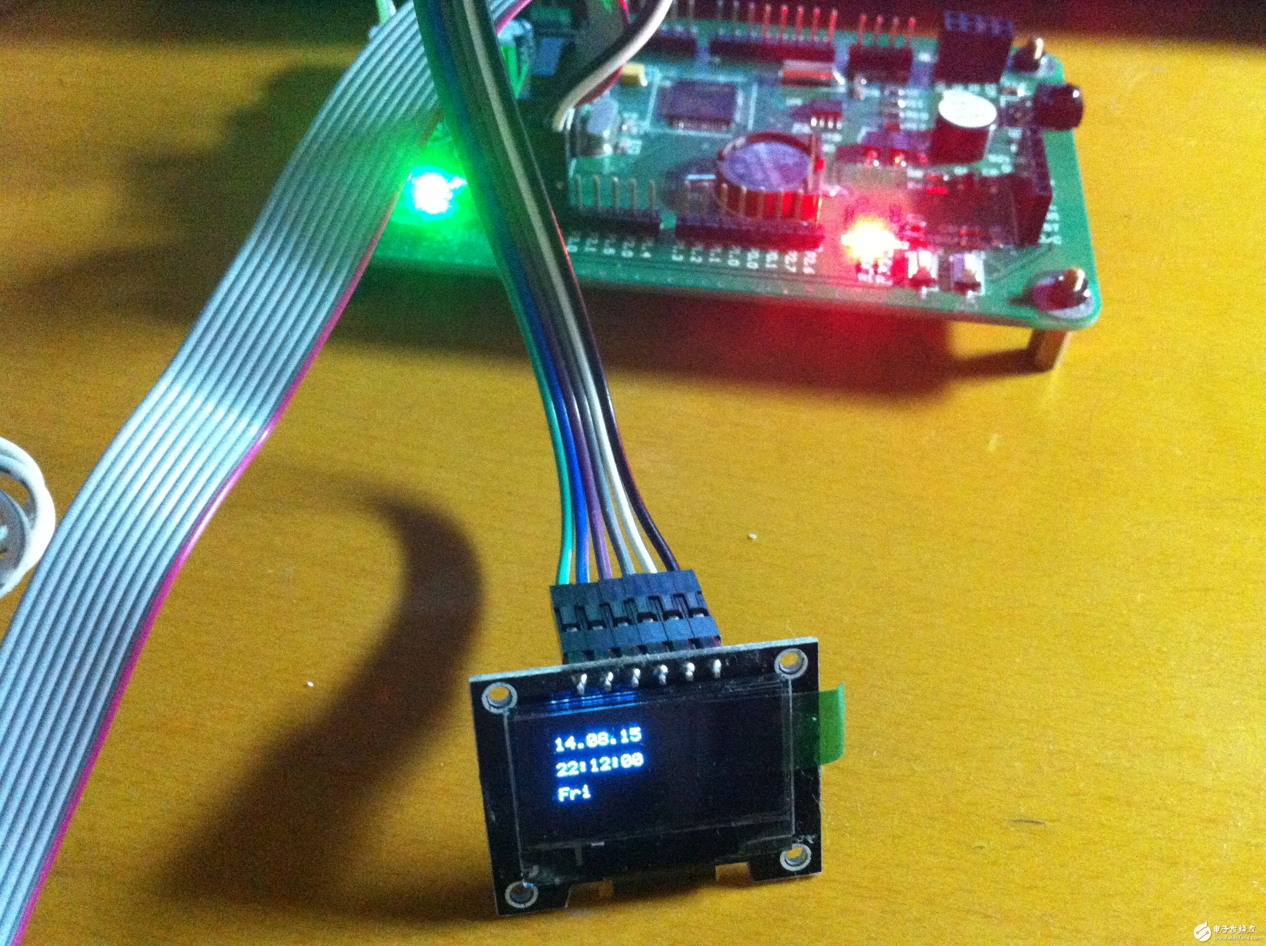
Rocker Switches
Rocker Switches is also called a boat switch, an IO switch, and a power switch. The structure of the rocker switch is the same as that of a Toggle Switches and Slide Switches, except that the handle of the rocker is replaced by a ship. This On Off Rocker Switches often used as the power switch of electronic equipment. Its contacts are divided into single-pole single-throw and double-pole double-throw, and some switches also have indicator lights.

It is a household circuit switch hardware product. Custom Rocker Switches are used in drinking fountains, treadmills, computer speakers, car batteries, motorcycles, plasma TVs, coffee pots, plugs, massage machines, etc., involving commonly used household appliances.

It can divided into Momentary Rocker Switch and square Rocker switches with plastic material,second two-foot boat switch, second three-legged boat switch, three-speed three-legged boat switch, three-speed six-legged boat switch, two-speed six-legged boat switch , round boat switch, square boat switch.
Rocker Switches,Round Rocker Switch,Carling Rocker Switch,Kenworth Rocker Switches
YESWITCH ELECTRONICS CO., LTD. , https://www.yeswitches.com