introduction
As a typical application of software radio, digital correlator has become an indispensable technology in spread spectrum communication. In traditional spread spectrum communication, analog devices (such as surface acoustic wave devices) are used to realize the despreading unit, and the use of digital correlators can increase the flexibility and stability of the system. Therefore, the research on digital correlators has more Great meaning. This article uses the structure of DSP + FPGA, on the one hand, it makes the design more flexible, and at the same time reduces the cost of production. In consideration of versatility, this article uses a zero-IF sampling system. It is proposed how to correctly convert the analog signal in the channel to the digital signal after passing the correct zero-IF sampling and digital correlator. This paper gives the digital related algorithms and simulation results, the algorithm flow chart implemented with DSP + FPGA, and finally gives the actual measurement results of the system.
Introduction to despreading algorithms
Signal model at the origin For digital signals, project them onto I and Q two orthogonal signals respectively, which have the same characteristics. Therefore, only the I signal is analyzed here, and the Q signal can be obtained in the same way.
After channel coding, channel I baseband information has a rate of 3.103 kb / s and a symbol interval of 323 μs, and then performs PN code spreading. The length of the PN code is 1 023 and the rate is 3.174 Mcps. Therefore, after spreading, channel I The baseband chip's speed rise is 3.174 Mcps, and the spreading gain is 30 dB. The signal can be expressed as:

Where an = ± 1, n ∈ (0, ∞) is the information code, ck is the spreading code, gTb (t) is the rectangular pulse, Tb = 310 ns (pulse shaping is not considered here, usually a raised cosine pulse should be used) .
Correlation peak acquisition and synchronous decision algorithm analysis and mathematical derivation are at the receiving end. The received QPSK signal is demodulated first. The demodulation uses coherent demodulation. First, the analog baseband waveform is sampled, and the resulting data stream is slidingly correlated. To get a relevant value. Due to the inherent characteristics of the PN code, when the local PN code is aligned with the correlation code in the data stream (synchronized), a high correlation peak can be obtained, while when it is not aligned (unsynchronized), the correlation value obtained is very small, which This feature reduces the possibility of misjudgment on the one hand and improves the anti-interference performance of the system on the other hand. The corresponding block diagram of demodulation and despreading is shown in Figure 1.

Figure 1 Despread and demodulation model at the receiving end
Assuming that the channel is a Gaussian white noise channel, there is only time delay, Gaussian white noise, and no multipath expansion, then the received signal r (t) and the originating signal s (t) have the following relationship:
Here, τ is the channel propagation delay, and n (t) is the channel noise. After multiplying the local carrier, the expression r′I (t) can be obtained as follows:
Since the local carrier is extracted by the received signal through a phase-locked loop, the carrier delay caused by the channel delay can also be captured, so cos ωc (t-τ) is used to represent the local carrier.
r′I (t) passes through a low-pass filter to obtain r I (t). For the convenience of discussion, it is assumed that the low-pass filter can filter out the frequency-doubling component, and the corresponding value in the passband is constant 2.
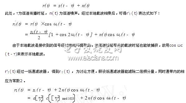
It can be seen that under ideal circumstances, the signal of the originating I channel can be recovered, and in fact the demodulation task has been completed. Next is AD sampling. Here, the AD sampling rate is set to 4 times the chip rate, which is equivalent to 4 signals for calculation when doing correlation. The advantage of doing this is that the best is selected every time. All the way to improve the receiving performance. In fact, the higher the sampling rate, the better the performance improvement, but it cannot be improved indefinitely, because the back-end digital devices have a processing power limitation. Since the processing of the four sampling signals in the digital despreading module is independent of each other, only one sampling signal is studied here. Since only one signal is studied, the sampling rate Ts can be equivalent to the chip rate. In this system, Ts = 1 / 3.1M.
Characteristics, the cross-correlation value is very small. It can be seen from the above formula that the second item is the main factor affecting the misjudgment. The discussion on the bit error rate here is different from the general sense of QPSK + spread spectrum. Therefore, the bit error rate will be discussed in a simulated manner.
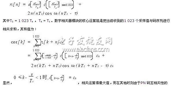
Using computer simulation, the bit error rate curve under Gaussian noise can be obtained as shown in Figure 2. From the simulation results, when SNR ≥-20 dB, it meets the requirements of voice communication (BER ≤10-3); when SNR ≥- 14 dB, it meets the requirements of data communication (BER ≤10-6).
Figure 2 Error performance of Gaussian channel
Algorithm Implementation in DSP + FPGA System
Since the digital related modules are mainly completed by FPGA and DSP, the main algorithm will be embedded in these two chips.
The biggest advantage of the DSP + FPGA system is its flexible structure and strong versatility. It is suitable for modular design and can improve the efficiency of the algorithm. At the same time, its development cycle is short, the system is easy to maintain and expand, and it is suitable for real-time signal processing.
In the real-time signal processing system, the low-level signal preprocessing has a large amount of data and high requirements for processing speed, but the operation structure is relatively simple. It is suitable for FPGA implementation hardware implementation, which can take into account both speed and flexibility. The characteristic of the high-level processing algorithm is that the amount of data processed is lower than that of the lower-level algorithm, but the control structure of the algorithm is complex. It is suitable for DSP chips with high operation speed, flexible addressing mode, and powerful communication mechanism.
The core of the DSP + FPGA system is composed of a DSP chip and a reconfigurable FPGA. It also includes some peripheral auxiliary circuits, such as memory, first-in first-out (FIFO) devices and FLASH ROM. The FPGA circuit is connected to the DSP, and uses the powerful I / O function of the DSP processor to realize the internal communication of the system. From a DSP perspective, FPGA is equivalent to his megafunction coprocessor. The peripheral circuit assists the core circuit to work. DSP and FPGA each have RAM, used to store the data and intermediate results required for the processing. FLASH ROM stores DSP executive program and FPGA configuration data. First-in-first-out (FIFO) devices are used to implement some operations commonly used in signal processing, such as delay lines and sequential storage.
In the design of this system, DSP uses C5409A of TI company, and uses AM29LV200BT of SPANSION company as the external FLASH of DSP to store the corresponding program; FPGA uses XCV600E of Xilinx company and XC18V00 of Xilinx company as the dedicated configuration chip , Store FPGA program; FIFO design will be carried out in FPGA, DSP reads the FIFO to realize the communication between the two chips.
The overall algorithm is divided into FPGA and DSP parts: FPGA's algorithm mainly includes the functions of generating AD sampling clock, receiving AD data, sliding correlation, FIFO composition and DSP interrupt generation; DSP contains: synchronization algorithm and decision algorithm.
The following is a schematic diagram of the algorithm embedded allocation in each chip, as shown in Figure 3.

Figure 3 Schematic diagram of the algorithm embedded in each chip
The algorithms of FPGA and DSP must work together. The relationship between them is: FPGA's algorithm is driven by the clock. When each clock arrives, he must receive the corresponding data, slide the correlation, and push the relevant value into the FIFO. Operation, when he sets the FIFO to a certain level, he sends an interrupt signal to the DSP; the DSP program is in a circular waiting state for most of the time, and as soon as he receives the FPGA interrupt, he responds, first Several data in the FIFO are read out, and then the corresponding interrupt processing is performed, and the DSP completes the synchronous processing, relevant judgment and baseband communication. The overall flow chart is shown in Figure 4.
Measured performance of system operation
During normal communication, the bit error rate is stable at 1 * 10-5. Gaussian noise interference (add interference before despreading and demodulation), the signal-to-interference ratio of normal communication of voice signals (bit error rate ≤1 & TImes; 10-3): -17dB. In terms of anti-interference, the signal-to-interference ratio of normal communication (bit error rate ≤1 & TImes; 10-3) for non-targeted single-frequency interference voice signals: -14 ~ -2dB (different with frequency point); When the single frequency interference reaches -12 dB, it can still maintain voice communication.
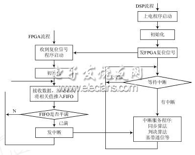
Figure 4 FPGA and DSP flow chart
Featuring level VI energy efficiency and meet IEC/EN/UL 62368 safety standards for ITE/AV equipment, the external universal Power Adapter accepts the output voltage ranging from 5 Volt to 36 Volt and provides 3 Years warranty. These 76 W to 100 W series power adapters use PC flame retardant material housing, all materials conform to the international environment protection standard. Protections for over voltage, over current and short circuit are also included.
76 ~ 100 Watt Desktop Adapters
RoHS Adaptor,Universal Ac/Dc Adapter,Power Ac Dc Adapter,Universal Power Supply Adapters,Power Adaptor Safety Mark
Shenzhenshi Zhenhuan Electronic Co Ltd , https://www.szzhpower.com