Integral integration (integraTIon-by-parts) is a concept that has been learned from the first grade of university. Now RF IC manufacturers are applying this traditional method to the integration of RF wireless circuits. Pioneer companies in the wireless IC field such as Analog Devices , RF Micro Devices, and Maxim continue to design and produce new building blocks (ICs) , and then create customized versions for specific customers or applications. Subsequently, these special devices were included in the standard product catalog. The products in these catalogs themselves have become the building blocks of more complex products. Digital IC manufacturers have been using this model since the 1960s . RFIC semiconductor manufacturers also adopted this model in the 1990s , resulting in a large number of RFIC companies and solutions.
Step-by-step integration actually means that the design cycle only needs to start with existing building blocks, create different versions, and then combine these building blocks into a more integrated circuit. The first wave of RF IC manufacturers successfully verified this business model.
RFIC companies have just developed, and soon ushered in the era of .com . At that time, it was relatively easy to raise funds (of course by today's standards ) , and fabless semiconductor companies became the preferred business model. Driven by university research support and the rapidly emerging standards such as Bluetooth, 802.11x, and OC-48 / 192 , these companies often pursue highly integrated communications products, such as RF or optical transceivers ( Figure 1) . Such companies have not adopted a step-by-step integration strategy. Instead, they usually focus on a unique application, and the goal of the effort is to make the company publicly listed or acquired. Although this approach was initially successful, several factors have combined to limit its further development. These factors include the bursting of the .com bubble, the economy falling into a severe and prolonged recession, and the traditional value of investment has been re-emphasized. After all, the bottom line of an enterprise is the most important. With the increase in integration and increasing global competition, the profits of RF ICs that support standards such as Bluetooth and 802.11 have become very thin. This is because everyone is competing for the limited RF IC chips in mobile phones ( Figure 2) . Due to the current overcapacity, we can imagine that this situation will be difficult to change for a while, so the price of these chipsets will be very cheap.
A large number of new companies are flooding into the limited market like Bluetooth or 802.11 . This makes the original business model that wins with technological advantages actually only maintain the advantage of about 6 months ( the average period of hardware updates ) , and will soon be surpassed by other companies. Too many seemingly successful and low barriers to entry quickly lead to excess production ( supply ) capacity. These companies ultimately have to make money by selling products, but their products are extremely profitable when sold in the consumer electronics market. In other words, this RFIC integrated business model almost collapsed. In addition, the global nature of the consumer electronics market makes knowledge of IC design alone insufficient to support a successful business. Intersil 's sale of its wireless local area network (WLAN) business, which holds a major market share, is a shocking event. This incident once again illustrates the difficulty of making money in the field of consumer electronics.
Peregrine initially tried to seize the development trend of .com , but Peregrine insisted on using the traditional method to develop the company's product line: that is, adopting the previous generation of step-by-step integrated business model. However, Peregrine 's approach is still different from tradition. Peregrine did not start its integration work from the baseband side of the radio frequency unit, but from the antenna side, first integrating functions that were originally dominated by gallium arsenide (GaAs) technology.
integrated
Integration can provide many benefits, such as reducing costs, reducing size, improving performance, reducing the number of devices, and related vendor management issues, while also adding functional features. In the 1980s and 1990s , digital circuits evolved from large-scale integration (LSI) to very large-scale integration (VLSI) , integrating the functions originally performed by discrete chips into single-chip devices. Technological advances, design tools and the development of high-volume markets are the main drivers. RF integration is still in its early stages, mainly because HDL methods for RF IC design have not yet been developed .
Nevertheless, RF IC integration has achieved outstanding results. In the past decade, the RF field has made tremendous progress, from traditional heterodyne high intermediate frequency (IF) and double conversion receivers to low intermediate frequency receivers, and then to direct conversion reception. Similarly, the demodulation process also began to use digital technology, using intermediate frequency sampling and multi-channel receiver technology. The transmitter has evolved from voltage-controlled oscillator (VCO) direct analog modulation to biased in-phase and quadrature (IQ) modulation, to direct-transmit IQ modulation. The new polarization modulation technology is becoming a universal transmission structure.
Many improvements in radio frequency structures have been around for decades, but the manufacturing process technology cannot support these methods. It seems that the changes have come out in the past few years, but the research has actually been carried out for many years. It's just that it took quite a long time for the advanced silicon manufacturing process to catch up.
Barriers to integration
The integration of mobile phone transceivers uses a variety of feasible technologies. In fact, the radio frequency front end of the mobile phone is still in a state of technological separation. This is mainly due to power amplifiers and related control circuits, switches, anti-static (ESD) protection and filters. One of the research focuses on using silicon technology to implement power amplifiers, whether it is silicon germanium (SiGe) , bipolar complementary metal oxide semiconductor (BiCMOS) or Bulk CMOS technology. Now, there is no problem to do this, but it does not match the performance of III-V compound semiconductors. The main problem is to reduce costs.
Once this circuit design obstacle is overcome, and the power amplifier (PA) is realized using silicon technology with reasonable efficiency , then another technical obstacle must be faced. That is to isolate the problem. It is difficult to ensure that the parasitic signal of the transceiver is not coupled to the PA output and the output signal of the transmitter in a frequency-multiplexed RF structure ( such as code division multiple access (CDMA) system ) . Isolation restrictions prevent further integration.
So why not put the RF part on the baseband chip? This is because it is difficult to ensure that digital circuits do not affect the operation of RF functions. Peregrine 's sapphire epi-silicon (silicon-on-sapphire) RF CMOS technology does not have the isolation limitations between conductive and semiconductor substrates faced by other silicon process technologies.
Gallium arsenide (GaAs) does work on semi-insulating substrates, but it lacks the complementary devices needed to achieve the level of integration required for silicon processes. Although GaAs has been used in many fields of RF and optoelectronic subsystems, it is now only used in high-performance front-end devices that silicon-based solutions cannot meet. However, even this last position, GaAs, seemed to be untenable. GaAs is quickly fading out. Due to the lack of complementary devices, GaAs integration potential is limited, which is also the reason for its bleak future development prospects. GaAs is also dominant in the microwave band, but also, silicon technology has made great progress in this regard. In mobile phones, GaAs is commonly used in power amplifiers and antenna switches. This situation is changing.
Peregrine 's RF CMOS device
Peregrine 's standard devices are building blocks that are manufactured in a step-by-step integration manner. These devices compete directly with silicon and III-V semiconductor devices in the industry . In terms of switches, Peregrine 's devices directly compete with mobile phone antenna switches, although GaAs devices have been in operation for at least 10 years. Peregrine also manufactures high isolation switches for the cable television (CATV) market. Single-chip switches like PE4256 can replace mechanical relays in CATV applications, which can support the deployment of remotely addressable CATV transmission systems and reduce the number of service and maintenance personnel.
The core of these switches can also be used for 5- and 6 -bit digital step attenuators with integrated serial and parallel interfaces . An additional benefit of Peregrine 's RF CMOS process is that it can preset power-on attenuation settings so that the device can be placed in a predetermined state before the microprocessor takes control of the device.
Market demand for integration
Peregrine has developed a series of single-pole multi-throw mobile phone antenna switches, using RF CMOS technology to obtain a 10W compression point. Unlike GaAs , Peregrine can integrate CMOS control logic. Peregrine also provides better ESD performance without the need to use capacitor arrays to raise the switch to positive control logic. Until now, GaAs amorphous high electron mobility transistors (pHEMT) and PIN diodes are the only technologies on the market that can meet performance requirements. Bipolar devices cannot make switches, while Bulk CMOS devices have problems with substrate insertion loss and meeting power requirements. For low insertion loss switches, low on-resistance is necessary. The following simple equation relates the insertion loss to the series resistance value.
IL = -10 * log ((4Rl ^ 2 / (Rs + Rl) ^ 2)
For switching devices, an important parameter is the Ron * Coff product value. That is, the on-resistance of the device is multiplied by the off-capacitance. By increasing the size of the device, the on-resistance of the device can be reduced, but the off-capacitance value increases at the same rate at this time, thereby reducing the available bandwidth and deteriorating high-frequency isolation. The switch made by Peregrine 's ultra-thin silicon (UTSi) RF CMOS technology has made rapid progress in improving Ron * Coff parameters. UTSi switches have made tremendous progress in the past three years, and more improvements are already on the agenda.
Since the performance of the SP4T ( single pole four throw ) switch manufactured in this way is comparable to GaAs , and the switch performance of a larger number of switches is better than GaAs , so with the trend of multi-mode and multi-band mobile phones, the complexity increases, RF CMOS technology will become more important. Since the multiplexer is basically the first device after the antenna, it can be used as the basis for integrating adjacent functions, such as filters, matching networks, power amplifiers (PA), and low-noise amplifiers (LNA) .
Peregrine 's development plan is to further integrate more functions, first of all is to integrate some functions that currently belong to the power amplifier module. The radio frequency, passive and digital circuits in the power amplifier module, including the bias circuit, output matching and power control circuit can be integrated into a single chip with the antenna switch. A fully insulated sapphire substrate can produce high quality factor passive devices without voltage coefficient or capacitive substrate coupling problems. EEPROM can be integrated without additional masking steps, so that the correction coefficient of the power amplifier can be stored locally. This E ^ 2 function has been applied to the PLL with integrated E ^ 2 , which is ideal for fixed frequency applications. The development plan includes integrating the amplifier driver, and a new type of power amplifier unit can be designed on this basis, and the E ^ 2 look-up table is used for pre-distortion or polarization modulation.
Since sapphire is transparent from the ultraviolet (UV) to infrared (IR) bands, the UTSi CMOS process is used to manufacture high-performance parallel optical interconnect devices.
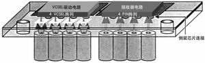
Picture 3 Â Flip chip based on UTSi
Figure 3 shows a 10 Gbps bidirectional ( transmit and receive ) parallel optical module manufactured using UTSi CMOS process . By flip chip connection of vertical cavity surface emitting laser (VCSEL) and PIN photodetector diode to the drive circuit ( laser drive circuit and TIA / LA) , almost all problems related to bonding parasitic parameters and alignment can be solved . Alignment positioning holes are cut by laser on the sapphire substrate to provide mechanical self-alignment function, thereby ensuring reliable optical coupling.
LED rental screen is a kind of Led Display screen specially used for mobile stage performance and artistic activity performance, with rich display content and all-weather use ability, which is more and more widely used. The LED rental display screen is generally designed as a custom-made die-casting aluminum box, which is light and thin, quick disassembly and convenient transportation, suitable for different areas of application places. It can be processed synchronously and asynchronously, and can accept the access of DV, VGA, dhmi, SDI video, 4K signal, composite yuy and other new signal sources. Video, picture and text can be played at will.

Mobile Led Screen features:
1. The light, thin and fast lock design of
the box body enables quick disassembly and assembly during use. It is equipped
with an aircraft box, safe and convenient transportation. The box body can be
equipped with arc lock and rotate the lock at ± 15 ° to meet the use
requirements of customers for different sites.
2.
Signal source: support any direction of signal source, meet the arrangement and
placement of different boxes, and create different effects and pictures.
3.
Levelness: the box body adopts die-casting aluminum structure, with high
precision, good flatness and no shadow.
4. The screen body is equipped with a video
processor, which can delay AV, VGA, DVI, HDMI, SDI and other signal sources to
achieve full screen, split screen, picture in picture, live broadcast and other
effects.
6. Heat dissipation effect: the box is made of aluminum material, which does not need built-in fan air conditioner, etc. to reduce the power consumption of the box and work more quietly.
7. cabinet size: now it is mainly used for LED rental panel box size of 500 * 1000mm, 500 * 500mm, 576mm * 575mm, 512mm * 512mm480 * 480mm and other standard boxes.

Application scenario: widely use stage
rental, press conference, stadium, 4S point, sales center, lecture hall,
multimedia video, hotel, conference room, etc.
Precautions:
the screen body is divided into indoor and outdoor, indoor screen body shall
not be exposed to rain, edges and corners shall not be collided, and shall be
handled gently.

Indoor Led Screen,Mobile Led Display,Led Display,Led Screen
Shenzhen Vision Display Technology Co,.LTD , https://www.ledvdi.com