Hotspot assault! The era of fast charging and unification is coming? A good opportunity with [Type-C & Fast Charge Technology Forum]
Fast charging technology is undoubtedly one of the key points for the development and promotion of smartphone manufacturers. Its solutions include Qualcomm's Quick Charge, MediaTek's Pump Express, and self-developed private technology. These technologies have different charging protocols and cannot be quickly charged to each other. With the popularity of the USB type-c interface, the Power Delivery (PD) protocol not only provides a unified fast charging standard for all electronic devices using type-c interfaces, including mobile phones, but also accelerates the development of battery direct charging solutions. universal. This paper combines the actual project to complete a complete mobile phone fast charging system based on PD protocol, including the hardware and software design of mobile phone and charger, flexible programmable charging protocol and perfect charging process. This program has been successfully applied to mobile phone products of well-known brands and achieved good results.
A PD charger hardware structure
The hardware structure of a typical mobile phone charger (take the Qualcomm QC2.0 fast charging protocol based on the Dialog scheme as an example) as shown in Figure 1. As the QC2.0 protocol controller, the iW626 conducts power supply negotiation via the D+/D- signal of the USB port and the AP on the mobile phone side, and then adjusts the output voltage by controlling the primary AC/DC controller iW1780 through the optocoupler.
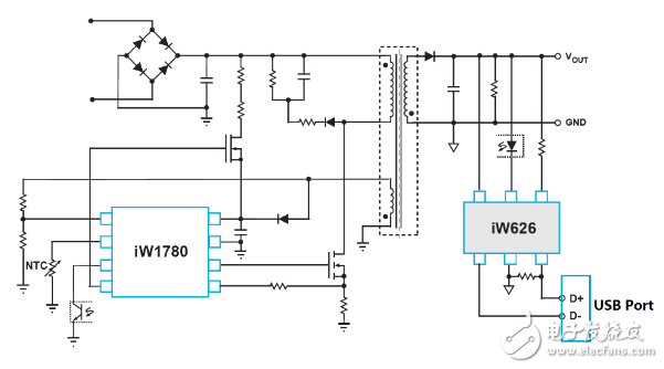
Figure 1 LOCK scheme based Qualcomm QC2.0 fast charge protocol charger hardware block diagram
The charger circuit based on the PD protocol can maintain the AC/DC part unchanged, but replaces the QC protocol controller with the PD controller [1], such as CCG2 (type-c Controller GeneraTIon 2) of Cypress Semiconductor. CCG2 is one of the first USB-IF-certified PD controllers. It includes an ARM® Cortex®-M0 processor and a complete PD protocol transceiver for chargers, mainframes, accessories, and EMAC cables. The application of -c port has many mass production cases in the first-line brand customers such as Apple, Lenovo, HP, Dell, Xiaomi and LeTV.
The schematic diagram of the charger circuit using CCG2PD controller and Dialog AC/DC controller is shown in Figure 2. CCG2 communicates with the mobile phone AP through the CC signal of the Type-C port, and then controls the voltage and current through the PWM control optocoupler. Demand feedback to AC/DC for output regulation. CCG2 will ensure the reliable operation of the PD protocol state machine by sampling VBUS, and control the on and off of VBUS through the MOSFET according to the PD state. In addition, CCG2 can also support the QC3.0 protocol through D+/D-, and realize the coexistence of PD and QC on the same Type-C port (the two can not be used at the same time in actual work, the user can define the priority and the enabling strategy). In addition to the voltage regulation charging, the PD fast charge can also perform current regulation to achieve current fine adjustment or high current charging or even direct charging. CCG2 can use the internal ADC for voltage and current sampling, closed loop control and OVP/OCP/UVP protection. The protection mechanism of CCG2 is software controlled, so it is not real-time enough to act as an auxiliary or redundant protection for AC/DC controllers. Cypress's third-generation PD controller CCG3 integrates internal hardware OCP/OVP protection mechanisms while streamlining BOM, improves ADC accuracy, and provides an optimal high-current direct charge solution, which has been started by multiple mobile phone customers. The evaluation design.
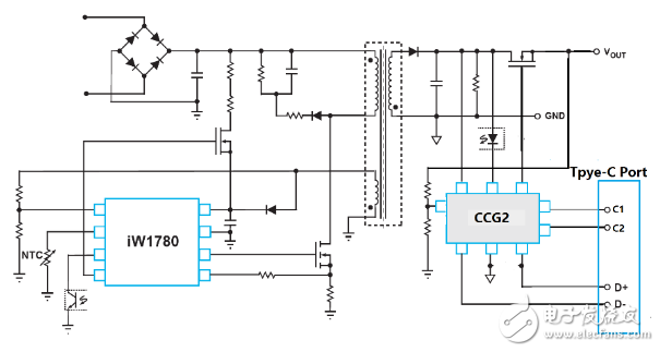
Figure 2 Charger hardware block diagram of PD and QC fast charge protocol based on Cypress CCG2 scheme
Two TYPE-C PD controller
This design uses Cypress's second-generation Type-C PD controller CCG2 on both the charger and the mobile phone side. The mobile phone side chip supports Dead Battery charging, and adopts a 1.6mm*2.0mm CSP package. The external device also has only a few resistors and capacitors, which saves the layout area [2]; the charger is packaged in QFN. The chip reduces the cost of patching and testing and solves the leakage problem of connecting the phone without 220V AC input. The CCG2 uses a 32-bit 48 MHz ARM® Cortex®-M0 processor with 32 KB of flash memory and a complete USB-PD subsystem, as shown in Figure 3. The subsystem includes a USB Type-C transceiver and physical layer logic, the transceiver performs BMC and 4b/5b encoding, decoding and 1.2 V front-end bias, and also integrates the termination resistors required to complete the TYPE-C connection. RP (DFP), RD (UFP), and RA (EMCA) eliminate the need for complex peripheral resistors or current source arrays. CCG2 can support all the protocols of PD2.0 and the protocol of PD3.0 in the charging field, which is enough for fast charging or direct charging. The high-precision SAR (Successive Approximation Register) ADC inside CCG2 can realize data acquisition for voltage and current, realize another stage of closed-loop control or monitoring before AC/DC, and realize perfect TYPE-C port power supply control solution.
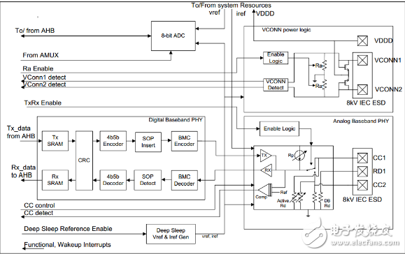
Figure 3 USB-PD subsystem of CCG2 controller
In addition, CCG2 uses Cypress's PSoC Programmable System on Chip, which integrates a rich array of configurable analog and digital peripheral devices around an MCU core, using the programmable interconnect array inside the chip. The embedded and digital resources on the chip can be configured intuitively and effectively according to actual needs to realize a customized embedded system. A single PSoC device can integrate hundreds of peripheral functions to help customers save design time and board space, reducing power and system cost.
Three PD charging software implementation
The PD charging system is divided into three levels from low to high: Type-C connection layer, PD protocol layer and charging strategy layer. The Type-C connection layer needs to ensure that the connection relationship between the Type-C devices is properly and stably established, and the negotiation process, role confirmation, and power supply output are repeated. The PD protocol layer provides links and specifications for communication between the two parties. The charging strategy is a core technology that requires mobile developers to design and continually optimize based on long-term experience accumulation and actual project testing. The charging strategy program can pass the voltage and current demand according to the battery, temperature and other information and the desired charging curve. It is transmitted to the PD layer through the HPI interface, and then transmitted to the charger through the Type-C CC signal and receives the charger feedback.
The charger software control flow based on PD protocol is shown in Figure 4. It mainly includes standard PD charging process, privatization charging process and voltage and current protection. The main program flow is shown in (a), including the initialization of the peripheral and the initialization of the subroutine. After the configuration is completed, the interrupt is enabled and the main loop is performed. The standard PD charging process is shown in (b). After the mobile phone is inserted into the charger as a powered device, after the data and power supply relationship determination is completed, the charger as the power supply device turns on the MOSFET output VBUS to 5V, and then broadcasts the power supply. ability. The mobile phone selects the voltage and current according to the defined power receiving capability, and the charger determines whether it can be satisfied according to the received power supply request, and then sends an acceptance or rejection message. If the charger can provide the voltage and current requested by the mobile phone, it will control the AC/DC to adjust the voltage and current capability of the output and set the corresponding voltage and current protection value. After the adjustment is completed, send the power supply ready information. The PD negotiated charging is complete.
After that, a customized privatization charging process for the product features of each handset factory can be initiated, as shown in (c). The privatization charging process is accomplished by the charger communicating with the mobile AP based on unstructured customized information (Unstructured VDM) or programmable PDO. For the sake of safety, before the private power supply negotiation, the design carries out the mutual identification of the charger and the mobile phone, and only the matching parties can perform the customized fast charging. Of course, as more and more devices support PD charging and the future of the PD protocol, privatized charging will be gradually replaced by a unified and flexible public charging negotiation mechanism to realize equipment of different types and different manufacturers. Adaptive, intelligent and efficient charging. After the privatization verification is completed, the mobile terminal initiates a data role exchange command (Date Role Swap), so that the mobile phone becomes the master device, giving full play to the advantages of the mobile phone AP processing capability and obtaining more information, according to the battery power, the system temperature. And the preset charging curve and other information, actively send the required voltage and current adjustment instructions to the charger. The charger adjusts the voltage and current according to the instructions on the mobile phone side and sets the corresponding protection value. After the adjustment is completed, the confirmation command is sent to the mobile phone to ensure the correct voltage and current adjustment.
Phone Case,Eco Phone Case,Cases For Phone,Popular Phone Case
Shenzhen Ruidian Technology CO., Ltd , https://www.wisonen.com