1 Introduction
The digital oscilloscope in the design of this paper is an improvement of the traditional high-speed electron beam oscilloscope. It can collect and store the measured periodic signal or single aperiodic signal, which is convenient for analyzing waveforms.
At present, there are already rich researches on digital oscilloscopes, but sometimes only low-end and mid-range digital oscilloscopes are required to achieve the standard in development and design. Aiming at this paper, a design scheme of a simple digital oscilloscope is given. The digital circuit is used as much as possible. The structure is simple and the measurement result is reliable and has high resolution and low error.
2. System design
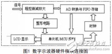
The design scheme adopts S12 single-chip microcomputer as the main control chip, and the signal-controlled amplification circuit passes the signal attenuation amplification, and then is sent to the FIFO chip through the TLC5510 sample for buffer storage and shaping circuit, and then S12 reads data from the FIFO, and processes the waveform and peak-to-peak value after processing. The display is performed on the LCD, and on the other hand, the S12 frequency is input from the shaping circuit, and the frequency is displayed on the liquid crystal panel.
2.1 Hardware Design
The hardware design includes program-controlled amplification, high-speed AD conversion and FIFO storage, clock circuit and power supply, shaping circuit and single-chip processing four circuit modules, the links between the modules are as follows:
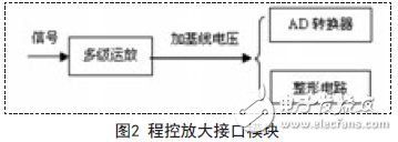
2.1.1 Program Control Amplifier Module
The function of program-controlled amplification is to attenuate or amplify the input signal so that the output signal voltage is within the input voltage requirements of the AD converter. The design uses the LM6172 op amp to form a multi-stage op amp to achieve signal scaling. The ULN2003 drives the electromagnetic relay, and the attenuation coefficient is determined by the single-chip microcomputer. Finally, add the baseline voltage (the midpoint of the AD converter input) to adjust the signal amplitude within the sampling range of the AD converter, send it to the AD chip for conversion and shaping, respectively perform AD conversion and convert the processed signal into a square wave signal for the MCU. Frequency measurement.
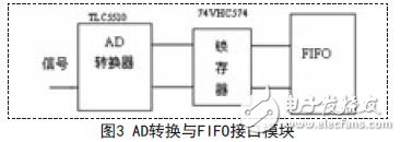
2.1.2 High Speed ​​AD Conversion and FIFO Memory Module
The AD converter samples the measured signal and converts it into a digital signal and stores it in the memory to determine the highest frequency that the digital oscilloscope can measure. According to the Nyquist theorem, the sampling frequency is at least twice the highest frequency of the measured signal to reproduce Signal measurement. In a digital oscilloscope, the sampling frequency should be at least 5~8 times the frequency of the measured signal to restore the waveform of the signal. In order to meet the acquisition of high frequency signals, an 8-bit TLC5510AD conversion chip was selected.
The FIFO (First In First Out Memory) acts as a high speed data buffer between the AD conversion and the microcontroller, with three flag pins FF (full flag), HF (half full flag), and EF (empty flag). According to these three flags, the MCU reads the data for processing when it is full, and disables the AD sampling clock. When half full, sampling continues, and when it is empty, it waits to read data. Since the AD conversion is faster, the 74VHC574 latch data can be added between the AD and the FIFO via the latch buffer and sent to the FIFO.
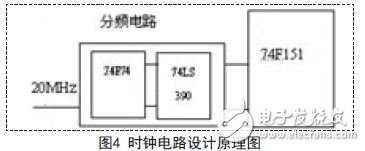
2.1.3 Clock Circuit and Power Module
The clock circuit provides the sampling clock signal for the AD converter. For the signal within 1MHz, the design is based on the 20MHz crystal oscillator, and the frequency dividing circuit composed of the counter obtains a series of different sampling periods, respectively 20MHz, 10MHz, 5MHz, 1MHz, There are 9 kinds of 500KHz, 100KHz, 10KHz, 1KHz and 500Hz, which correspond to different horizontal sweep speeds. A different sampling clock is selected by the microcontroller through the data selector 74F151 for the AD conversion sampling signal.
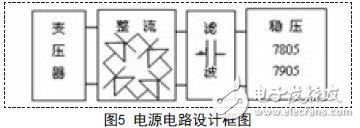
In order to achieve the purpose of simplicity and convenience, each module of this design is powered by ±5V power supply. The power module converts 220V AC power through the transformer and then converts it into ±5V DC voltage regulation by rectification, filtering and voltage regulation. Put, so use ±5V dual power supply, other modules +5V regulated source can meet the requirements.
TOMUU DC Solar Tracker Electric Linear Actuators are a powerful Electric Linear Movement Actuator, designed for Solar Tracker and other industry field. It features high load capability, long lifetime and low power consumption. The adjustable limit cam is convenient for the user to fine-tune the stroke, and moreover, the optical encoder possesses high resolution of stroke feedback, which is helpful on stroke control. Ball screw or ACME screw threaded spindle is available.

Solar Tracker Actuator,Solar Tracker Linear Actuator,24V Solar Tracker Actuator,Electric Solar Tracker Actuator
TOMUU (DONGGUAN) ACTUATOR TECHNOLOGY CO., LTD. , http://www.tomuu.com