This paper introduces the hardware part of the inverter power supply quality and reliability improvement design. The control method of the inverter power supply is not unique. Each control method has its advantages and disadvantages. How to skillfully integrate different control methods to get the best power quality is the designer's constant pursuit.
With the popularization of inverter power sources in power plants, substations and other institutions, the inverter power supply is dealing with the AC load of the UPS power supply more and more, and people have higher and higher requirements for processing efficiency. Therefore, increasing the power quality and power supply reliability of the inverter power supply has become the focus of designers' research and development. In this article, Xiaobian will introduce the hardware part of the inverter power supply quality and reliability improvement design.
There are many parallel strategies for inverter power supply. There is a master-slave structure. The voltage type inverter is used as the main module to control the system voltage, and the current type inverter provides the load current. There is a peer-to-peer equation. The parallel inverters have the same structure and signal transmission with each other, but there is no membership relationship. There is also a non-connected parallel connection based on active and reactive power regulation.
With the development of control technology, the emergence of high-speed digital processing chip DSP, achieving high-quality AC output has not been a problem. However, how to realize the redundant design of the inverter is still the main problem that plagues the developers. At present, the parallel technology of the inverter popular in the market is to use the system monitor to uniformly generate the SPWM signal for synchronization and load sharing. The technical disadvantage of the transformer is that the single inverter cannot work and must be equipped with the monitor of the system to work, so the performance and price ratio of the small system is not high. The reliability of the system depends on the reliability of the system monitor. Once the monitor is damaged, the whole system will be paralyzed; the AC output cannot be short-circuited, and the short circuit will cause the inverter to burn out.
No main parallel parallel inverter control mode
The scheme adopts a combination of various control methods, and a new principle design combining self-synchronization and external synchronization, which has the advantages of high reliability. It can be used in stand-alone or group screen, and it is easy to configure. The electronic switch plug-in method is adopted to facilitate the formation of other forms of inverter power such as UPS and EPS. The system monitors three synchronous signals that can be phase-shifted by 120 degrees, which are convenient to be combined into a three-phase inverter power system; and the three phases are individually adjusted, and each phase can carry 100% unbalanced load.
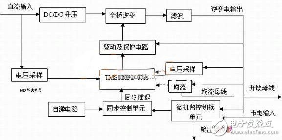
Figure 1 system principle box
Hardware design part
The parallel circuit module hardware circuit is composed of power processing main circuit, control drive circuit and protection circuit. The system block diagram is shown in Figure 1. The DC/DC converter circuit is BOOST circuit. The high frequency loop is used for inverter, so there is no need to use power frequency transformer. The volume is reduced, and the function is to convert the DC 220V voltage into the voltage required by the PWM rectification inverter circuit by using the DC-DC full-bridge high-frequency isolation boost for the full-bridge inverter of the latter stage, and the control system results are as follows. Figure 2 shows. After the output given current Ug is compared with the actual output voltage Uk, the error signal is compared with the sawtooth wave by the PI regulator to form a PWM signal, and the signal is then controlled by the driving circuit to control the switching device IGBT in the BOOST circuit. The actual output voltage tracks a given voltage. This system uses the PWM controller SG3525 to obtain the PWM control signal.
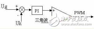
Figure 2 DC / DC converter circuit control structure
The power processing of the inverter adopts a full-bridge circuit. After SPWM modulation, the output is filtered by the filter inductor and capacitor, and directly connected with the output of other inverters. When the requirements and the power grid are quickly switched, the system main monitoring command The switching action of the electronic switching box realizes the bypass switching with the power grid.
The control circuit DSP TMS320F2407A completes the functions of SPWM waveform generation, phase lock, control, current sharing, synchronous signal capture, and data sampling. The output voltage feedback signal is sampled by the analog/digital conversion module inside the DSP, and the voltage effective value outer loop control is completed by the digital PI controller to ensure that the output voltage RMS is stable. The output of the PI controller is multiplied by a standard reference signal, which is used as a reference input signal for the analog part of the control circuit after digital/analog conversion.
The master-slave setting method and the average current method cannot implement the redundancy technology, so the reliability of the parallel power module system is not well guaranteed. The UC3902 adopts the independent current sharing chip according to the unique performance, such as: "high current sharing precision, good dynamic response, redundancy technology, etc.", the independent current sharing method is essentially in N parallel modules, the output current is the largest. The module will automatically become the main module, and the remaining modules will become slave modules. The voltage errors of each slave module will be adjusted in order to adjust the imbalance of load current distribution. Since N parallel modules have no artificially set which module is the main module, but are randomly sorted according to the magnitude of the output current, the module with a large output current automatically becomes the main module. The control system adopts the chip to directly obtain the current sharing error signal, which simplifies the complicated current calculation of the control system and improves the system reliability.
The UC3902 integrated chip matches all of the output current by precisely adjusting the output voltage of the converter. In addition, this chip has a unique advantage that the differential mode is used to load the busbar. This structure greatly enhances the system's ability to suppress noise. The UC3902 current sharing chip has the following features in the power supply: (1) High current sharing accuracy. (2) The peripheral circuit design is simple and not too complicated as UC3907. (3) Easy to do hot swap operation.
Our banknote handling machines mainly include following
BC -30: basic piece counter with only one UV
BC-35: piece counter with UV MG
BC-40: value counter with one CIS, support 4 currencies, Auto recognition, multi-currency mix counting
BC-55: value counter with two CIS, support 40 currencies at the same time, serial number reading, Auto recognition, multi-currency mix counting, remote software upgrading via network
Those 4 models have similar structure, passage can be opened from reat side, easy for maintenance and cleaning
BCS-160: 1+1 Pockets Banknote Sorter with two CIS, support 20 currencies at most, serial number reading
Euro Banknote Sorter,1+1 Pockets Banknote Sorter,Two Pockets Banknote Sorter,Banknote Sorter
Suzhou Ribao Technology Co. Ltd. , https://www.ribaoeurope.com