Abstract: The Dallas Semiconductor DS2155 or DS21455 single-chip transceiver (SCT) can be used to create an interface that is compaTIble with the Japanese JJ-20.11 standard. Both the DS2155 and DS21455 have a digital mulTIplexer and I / O interface that provide access to the clock and bipolar data signals between the framer and LIU secTIons. Using a FPGA or CPLD, the data steam can be modified to support the JJ-20.11 standard. Because the LIU already has the ability to code and decode the Coded Mark Inversion ( CMI) signal used in JJ-20.11, only a slight modificaTIon is needed to increase the gain of the receive signal.
IntroductionThis application note describes how the Dallas Semiconductor DS2155 or DS21455 single-chip transceiver (SCT) can be used to create an interface that is compatible with the Japanese JJ-20.11 standard. The JJ-20.11 standard describes the electrical and physical conditions used by Japanese private branch exchange (PBX) systems conforming to the JJ-20.10 standard. Both the DS2155 and DS21455 have a digital multiplexer and I / O interface that provide access to the clock and bipolar data signals between the framer and LIU sections. See Figure 1. Controlling the data flow to the I / O signals is simple, and can be performed in software with the LBCR.LIUC register bit and / or in hardware with the LIUC pin. Using a FPGA or CPLD, the data steam can be modified to support the JJ-20.11 standard. Because the LIU can code and decode the Coded Mark Inversion (CMI) signal used in JJ-20.11, only a slight modification is needed to increase the gain of the receive signal. The following informatio n and detailed diagrams explain all the changes necessary to support the JJ-20.11 standard.
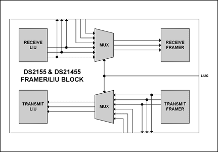
Figure 1. Simplified block diagram of DS2155 transceiver. Receive-Side DesignThe JJ-20.11 standard uses a code violation of the CMI coding scheme to indicate the first bit of the 256 bit frame. The receive-external circuit, Figure 7 in the Appendix, monitors the RPOSO and RNEGO signals and detect the CMI bipolar violation (BPV), which initiates the delay counter. RPOSO and RNEGO are then combined into a unipolar data stream and passed through an 8-bit shift register. When the counter reaches 129 (the start of JJ-20.11 Time Slot 16) it causes the shift registers to alternately load the E1 frame alignment signal (FAS) and nonframe alignment signal (NFAS) patterns into Time Slot 16, thus overwriting the unused portion of the JJ-20.11 data stream . The modified data stream is then input simultaneously at the RPOSI and RNEGI, which allows the framer to operate in unipolar mode. Figure 2 details the receive-side data-stream bit timing after being modified by the external circuitry.
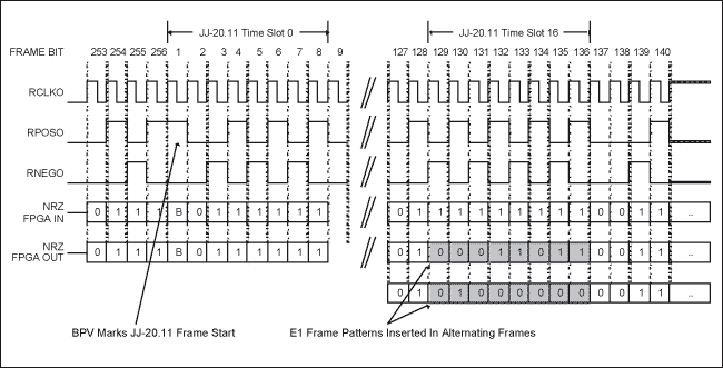
Figure 2. Receive synchronization framing and bit position information.
Because the FAS / NFAS pattern is inserted into Time Slot 16 of the data stream, the framer will align to this pattern, effectively moving all the JJ-20.11 time slots forward 16 channels. As a result, the JJ-20.11 frame pattern from Time Slot 0 is shifted to Time Slot 16, allowing the multiframe alignment, alarm indication, and signaling bits to be read with the internal framer registers, RS1 through RS16. Because the framer's internal register space is twice as large as the JJ-20.11 multiframe, these registers will actually hold two consecutive multiframes of JJ-20.11 information. The software only needs to locate the zero in the third bit of the registers, which indicates the multiframe alignment of the JJ-20.11 frame pattern.
Because the time slots have shifted forward 16 channels, the external devices must account for this time shift. These devices include any connected to the framer's receive serial data (RSER) or receive sync signal (RSYNC). Table 1 shows the shift pattern and the position of each time slot relative to the JJ-20.11 standard. This time-slot shift should not pose a problem as the standard was designed for PBX systems that usually only carry voice traffic. Because the voice data is normally piped into PCM codec devices for conversion to analog telephone lines, the system operator can arbitrarily number these lines. If it were necessary to restore the original time-slot mapping relative to the RSYNC pulse, the FPGA or CPLD logic already present could perform this function. A simple delay counter to shift the RSYNC pulse by 128 bits would restore all time slots to the original position.
Table 1. Receive Time Slot Mapping after Altering Frame Alignment
Transmit-Side DesignThe JJ-20.11 synchronization, alarm indication, and signaling bit information can be inserted into the data stream by transmit signaling registers TS1 through TS16 when the transmitter is in E1 mode. Alternatively, the JJ-20.11 Time Slot 0 could be inserted externally at TSER, which would require extra hardware. That procedure is not discussed here. Because the framer will insert the contents of these registers into Time Slot 16, the user needs to offset the data at TSER by 16 channels. This half-frame offset ensures that the contents of the signaling registers will actually be mapped into JJ-20.11 Time Slot 0 after the external FPGA or CPLD modifies the data stream. To perform the shift, the TCHBLK pin is programmed to go active during Time Slot 16, as shown in Figure 3.
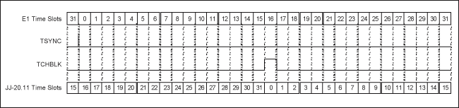
Figure 3. Transmit-side backplane timing.
The TCHBLK signal serves a dual purpose in the system. Firstly, the external circuit uses it to modify the TPOSO and TNEGO signals to generate the BPV, which indicates the first bit of the JJ-20.11 frame. Secondly, it is used to indicate the start of the JJ-20.11 frame so that the data at TSER can be properly aligned. In software, the TSYNC pin needs to be programmed as an output using the IOCR1.TSIO register bit, and TCHBLK needs to be programmed to go high during Time Slot 16 using the TCBR3.CH17 register bit. (Note that Time Slot 16 is also Channel 17 because of numbering conventions used in various specifications.)
The transmit external circuit, Figure 8 in the Appendix, delays the TCHBLK signal to account for the internal delay between the TSER input and the TPOSO and TNEGO output. Once the delayed TCHBLK goes high to indicate the start of the JJ-20.11 frame, the toggle flip-flop is tripped causing a change in the TPOSO and TNEGO mapping. Normally the TPOSO output is connected to the TPOSI input and the TNEGO output is connected to the TNEGI input, thus allowing data to flow to the line interface unit (LIU) unaltered. However, a change in the flip-flop state connects TPOSO to TNEGI and TNEGO to TPOSI. Another subsequent change in flip-flop state will restore the original mapping. While the change in mappingdoes not affect the data flow, it does cause the the ones pulse immediately following the change of state to be transmitted in the same polarity as the previous ones pulse. This results in a BPV, which is used to indicate the beginning of the JJ-20.11 frame. Figure 4 details the transmit-side data -stream bit timing after modification by the external circuitry.
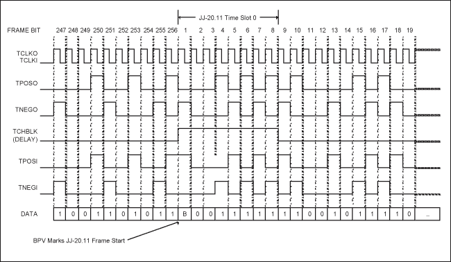
Figure 4. Transmit-side framer to LIU timing.
Because the time slots have shifted forward 16 channels, the external devices must account for this time shift. Those devices include any connected to the framer's transmit serial data (TSER) or transmit sync signal (TSYNC). Table 2 shows the shift pattern and the position of each time slot relative to the JJ-20.11 standard. This time-slot shift should not pose a problem as the standard was designed for PBX systems that usually only carry voice traffic. Because the voice data is normally supplied by PCM codec devices after conversion from analog telephone lines, the system operator can arbitrarily number these lines. If it were necessary to restore the original time-slot mapping relative to the TSYNC pulse, the FPGA or CPLD logic already present could perform this function. A simple delay counter to shift the TSYNC pulse by 128 bits would restore all time slots to the original position.
Table 2. Transmit Time-Slot Mapping after Altering Frame Alignment
Network Interface DesignThe network interface shown in Figure 5 is straightforward and only needs a couple of passive components and a comparator for transmitting and receiving a JJ-20.11 compliant signal. The transmit interface is extremely simple, as the TTIP driver is strong enough to produce the necessary output pulse into the 1: 1 transformer.
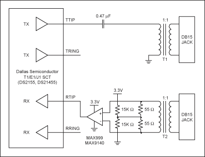
Figure 5. Illustration of a network interface circuit.
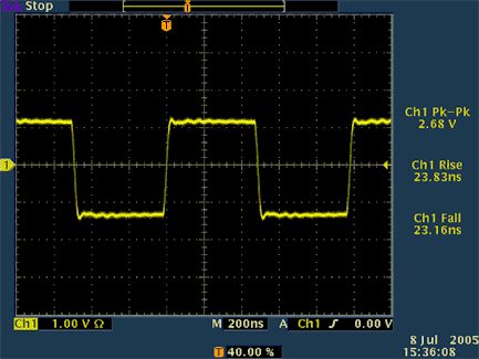
Figure 6. CMI pulse transmitted into 110Ω termination load.
Figure 6 shows a scope plot of the transmit output being driven into a 110Ω load. While signal amplitude is slightly low, it meets the 3.0V ± 0.75VP-P standard. If an increase in the output-signal amplitude is desired, changing the transformer winding to 1: 1.15 sets the amplitude to exactly 3.0VP-P.
The receive interface requires a comparator because the RTIP pin is only capable of decoding a CMI encoded signal at the normal CMOS voltage level. JJ-20.11 states, however, that normal reception should be possible with a maximum cable loss of 13dB. At the lowest specified transmit output level of 2.25VP-P, the recovered signal would be approximately 0.5VP-Pand much too low to trigger the high threshold voltage of the CMOS input. While almost any high-speed single-voltage-rail comparator can be used in the circuit, the MAX999 or MAX9140 comparators are good choices. Both devices come in a small 5-pin SOT23 package, operate at high speed, and draw very little power. The remaining external components terminate the line and bias the comparator. The two 55Ω resistors appear to the line as a 110Ω load that minimizes reflections. The two 15kΩ resistors bias the incoming signal from the line so that the comparator works well below the necessary minimum-specified voltage. Software Register ProgrammingThe software design is straightforward and does not require any processor-intensive operations. When the SCT reset is complete, initialization is performed by writing to a small number of registers. The last registers that should be initialized are TS1 through TS16. These registers hold the JJ-20.11 frame structure and should contain neutral values. Because there are multiple standards for using the bits inside of the multiframe structure, the exact bit settings are not covered in this document. It is important to note, however, that the JJ-20.11 frame structure is only eight frames long, so registers TS9 through TS16 should simply contain a copy of the data in registers TS1 through TS8. A short example of the register initialization follows in Table 3.
Table 3. Example Register Initialization
* Only necessary if LIUC pin is in the HIGH state.
Once the SCT is initialized, the software only has to monitor the RS1 through RS16 registers for new alarm status and reconfigure the TS1 through TS8 (with data copies to TS9 through TS16) registers to indicate any alarm conditions. While monitoring RS1 through RS16, the software must check bit 2 of the data for the presence of the multiframe indicator because the RS1 register might not align to the start of the multiframe. This action will add some work for the processor, but it is easily overcome in a simple register remapping or data-copy routine. The data in the transmit registers and receive registers will be updated every two multiframes, as indicated by the TMF and RMF bits in Status Register 4. A few software functions may need to be implemented for channel idling, channel monitoring, or loopback and test operations.
For any additional questions or comments, please see the references at the end of this document. Appendix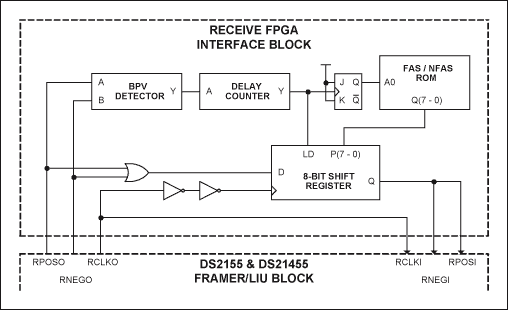
Figure 7. Diagram of a receive synchronization circuit.
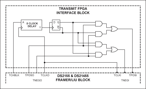
Figure 8. Diagram of a transmit bipolar violation generator.
References
For further questions on the JJ-20.11 interface design, please contact the Telecommunication Applications support team by email, var name = "telecom.support @"; var domain = "maxim-ic.com"; document.write ("" + name + domain + ""); telecom., or telephone in the USA at 972-371-6555.
More information and the product data sheets for the DS2155 or DS21455 SCT are available on the company's website.
IntroductionThis application note describes how the Dallas Semiconductor DS2155 or DS21455 single-chip transceiver (SCT) can be used to create an interface that is compatible with the Japanese JJ-20.11 standard. The JJ-20.11 standard describes the electrical and physical conditions used by Japanese private branch exchange (PBX) systems conforming to the JJ-20.10 standard. Both the DS2155 and DS21455 have a digital multiplexer and I / O interface that provide access to the clock and bipolar data signals between the framer and LIU sections. See Figure 1. Controlling the data flow to the I / O signals is simple, and can be performed in software with the LBCR.LIUC register bit and / or in hardware with the LIUC pin. Using a FPGA or CPLD, the data steam can be modified to support the JJ-20.11 standard. Because the LIU can code and decode the Coded Mark Inversion (CMI) signal used in JJ-20.11, only a slight modification is needed to increase the gain of the receive signal. The following informatio n and detailed diagrams explain all the changes necessary to support the JJ-20.11 standard.
Figure 1. Simplified block diagram of DS2155 transceiver. Receive-Side DesignThe JJ-20.11 standard uses a code violation of the CMI coding scheme to indicate the first bit of the 256 bit frame. The receive-external circuit, Figure 7 in the Appendix, monitors the RPOSO and RNEGO signals and detect the CMI bipolar violation (BPV), which initiates the delay counter. RPOSO and RNEGO are then combined into a unipolar data stream and passed through an 8-bit shift register. When the counter reaches 129 (the start of JJ-20.11 Time Slot 16) it causes the shift registers to alternately load the E1 frame alignment signal (FAS) and nonframe alignment signal (NFAS) patterns into Time Slot 16, thus overwriting the unused portion of the JJ-20.11 data stream . The modified data stream is then input simultaneously at the RPOSI and RNEGI, which allows the framer to operate in unipolar mode. Figure 2 details the receive-side data-stream bit timing after being modified by the external circuitry.
Figure 2. Receive synchronization framing and bit position information.
Because the FAS / NFAS pattern is inserted into Time Slot 16 of the data stream, the framer will align to this pattern, effectively moving all the JJ-20.11 time slots forward 16 channels. As a result, the JJ-20.11 frame pattern from Time Slot 0 is shifted to Time Slot 16, allowing the multiframe alignment, alarm indication, and signaling bits to be read with the internal framer registers, RS1 through RS16. Because the framer's internal register space is twice as large as the JJ-20.11 multiframe, these registers will actually hold two consecutive multiframes of JJ-20.11 information. The software only needs to locate the zero in the third bit of the registers, which indicates the multiframe alignment of the JJ-20.11 frame pattern.
Because the time slots have shifted forward 16 channels, the external devices must account for this time shift. These devices include any connected to the framer's receive serial data (RSER) or receive sync signal (RSYNC). Table 1 shows the shift pattern and the position of each time slot relative to the JJ-20.11 standard. This time-slot shift should not pose a problem as the standard was designed for PBX systems that usually only carry voice traffic. Because the voice data is normally piped into PCM codec devices for conversion to analog telephone lines, the system operator can arbitrarily number these lines. If it were necessary to restore the original time-slot mapping relative to the RSYNC pulse, the FPGA or CPLD logic already present could perform this function. A simple delay counter to shift the RSYNC pulse by 128 bits would restore all time slots to the original position.
Table 1. Receive Time Slot Mapping after Altering Frame Alignment
| Data Location | Frame | |||||||||||||||
| RPOSO / RNEGO Output | 0 (JJ-20.11 Sync) | 1 | 2 | 3 | 4 | 5 | 6 | 7 | 8 | 9 | 10 | 11 | 12 | 13 | 14 | 15 |
| RPOSI / RNEGI Input | 0 (JJ-20.11 Sync) | 1 | 2 | 3 | 4 | 5 | 6 | 7 | 8 | 9 | 10 | 11 | 12 | 13 | 14 | 15 |
| Receive Framer Internal | 16 (JJ-20.11 Sync) | 17 | 18 | 19 | 20 | twenty one | twenty two | twenty three | twenty four | 25 | 26 | 27 | 28 | 29 | 30 | 31 |
| RSER and RSYNC Output | 16 (JJ-20.11 Sync) | 17 | 18 | 19 | 20 | twenty one | twenty two | twenty three | twenty four | 25 | 26 | 27 | 28 | 29 | 30 | 31 |
| RPOSO / RNEGO Output | 16 (JJ-20.11 Empty) | 17 | 18 | 19 | 20 | twenty one | twenty two | twenty three | twenty four | 25 | 26 | 27 | 28 | 29 | 30 | 31 |
| RPOSI / RNEGI Input | 16 (E1 Sync) | 17 | 18 | 19 | 20 | twenty one | twenty two | twenty three | twenty four | 25 | 26 | 27 | 28 | 29 | 30 | 31 |
| Receive Framer Internal | 0 (E1 Sync) | 1 | 2 | 3 | 4 | 5 | 6 | 7 | 8 | 9 | 10 | 11 | 12 | 13 | 14 | 15 |
| RSER and RSYNC Output | 0 (E1 Sync) | 1 | 2 | 3 | 4 | 5 | 6 | 7 | 8 | 9 | 10 | 11 | 12 | 13 | 14 | 15 |
Figure 3. Transmit-side backplane timing.
The TCHBLK signal serves a dual purpose in the system. Firstly, the external circuit uses it to modify the TPOSO and TNEGO signals to generate the BPV, which indicates the first bit of the JJ-20.11 frame. Secondly, it is used to indicate the start of the JJ-20.11 frame so that the data at TSER can be properly aligned. In software, the TSYNC pin needs to be programmed as an output using the IOCR1.TSIO register bit, and TCHBLK needs to be programmed to go high during Time Slot 16 using the TCBR3.CH17 register bit. (Note that Time Slot 16 is also Channel 17 because of numbering conventions used in various specifications.)
The transmit external circuit, Figure 8 in the Appendix, delays the TCHBLK signal to account for the internal delay between the TSER input and the TPOSO and TNEGO output. Once the delayed TCHBLK goes high to indicate the start of the JJ-20.11 frame, the toggle flip-flop is tripped causing a change in the TPOSO and TNEGO mapping. Normally the TPOSO output is connected to the TPOSI input and the TNEGO output is connected to the TNEGI input, thus allowing data to flow to the line interface unit (LIU) unaltered. However, a change in the flip-flop state connects TPOSO to TNEGI and TNEGO to TPOSI. Another subsequent change in flip-flop state will restore the original mapping. While the change in mappingdoes not affect the data flow, it does cause the the ones pulse immediately following the change of state to be transmitted in the same polarity as the previous ones pulse. This results in a BPV, which is used to indicate the beginning of the JJ-20.11 frame. Figure 4 details the transmit-side data -stream bit timing after modification by the external circuitry.
Figure 4. Transmit-side framer to LIU timing.
Because the time slots have shifted forward 16 channels, the external devices must account for this time shift. Those devices include any connected to the framer's transmit serial data (TSER) or transmit sync signal (TSYNC). Table 2 shows the shift pattern and the position of each time slot relative to the JJ-20.11 standard. This time-slot shift should not pose a problem as the standard was designed for PBX systems that usually only carry voice traffic. Because the voice data is normally supplied by PCM codec devices after conversion from analog telephone lines, the system operator can arbitrarily number these lines. If it were necessary to restore the original time-slot mapping relative to the TSYNC pulse, the FPGA or CPLD logic already present could perform this function. A simple delay counter to shift the TSYNC pulse by 128 bits would restore all time slots to the original position.
Table 2. Transmit Time-Slot Mapping after Altering Frame Alignment
| Data Location | Frame | |||||||||||||||
| TSER and TSYNC Input | 0 (E1 Sync) | 1 | 2 | 3 | 4 | 5 | 6 | 7 | 8 | 9 | 10 | 11 | 12 | 13 | 14 | 15 |
| Transmit Framer Internal | 0 (E1 Sync) | 1 | 2 | 3 | 4 | 5 | 6 | 7 | 8 | 9 | 10 | 11 | 12 | 13 | 14 | 15 |
| TPOSO / TNEGO Output | 16 (E1 Sync) | 17 | 18 | 19 | 20 | twenty one | twenty two | twenty three | twenty four | 25 | 26 | 27 | 28 | 29 | 30 | 31 |
| TPOSI / TNEGI Input | 16 (JJ-20.11 Empty) | 17 | 18 | 19 | 20 | twenty one | twenty two | twenty three | twenty four | 25 | 26 | 27 | 28 | 29 | 30 | 31 |
| TSER and TSYNC Input | 16 (E1 Empty) | 17 | 18 | 19 | 20 | twenty one | twenty two | twenty three | twenty four | 25 | 26 | 27 | 28 | 29 | 30 | 31 |
| Transmit Framer Internal | 16 (JJ-20.11 Sync) | 17 | 18 | 19 | 20 | twenty one | twenty two | twenty three | twenty four | 25 | 26 | 27 | 28 | 29 | 30 | 31 |
| TPOSO / TNEGO Output | 0 (JJ-20.11 Sync) | 1 | 2 | 3 | 4 | 5 | 6 | 7 | 8 | 9 | 10 | 11 | 12 | 13 | 14 | 15 |
| TPOSI / TNEGI Input | 0 (JJ-20.11 Sync) | 1 | 2 | 3 | 4 | 5 | 6 | 7 | 8 | 9 | 10 | 11 | 12 | 13 | 14 | 15 |
Figure 5. Illustration of a network interface circuit.
Figure 6. CMI pulse transmitted into 110Ω termination load.
Figure 6 shows a scope plot of the transmit output being driven into a 110Ω load. While signal amplitude is slightly low, it meets the 3.0V ± 0.75VP-P standard. If an increase in the output-signal amplitude is desired, changing the transformer winding to 1: 1.15 sets the amplitude to exactly 3.0VP-P.
The receive interface requires a comparator because the RTIP pin is only capable of decoding a CMI encoded signal at the normal CMOS voltage level. JJ-20.11 states, however, that normal reception should be possible with a maximum cable loss of 13dB. At the lowest specified transmit output level of 2.25VP-P, the recovered signal would be approximately 0.5VP-Pand much too low to trigger the high threshold voltage of the CMOS input. While almost any high-speed single-voltage-rail comparator can be used in the circuit, the MAX999 or MAX9140 comparators are good choices. Both devices come in a small 5-pin SOT23 package, operate at high speed, and draw very little power. The remaining external components terminate the line and bias the comparator. The two 55Ω resistors appear to the line as a 110Ω load that minimizes reflections. The two 15kΩ resistors bias the incoming signal from the line so that the comparator works well below the necessary minimum-specified voltage. Software Register ProgrammingThe software design is straightforward and does not require any processor-intensive operations. When the SCT reset is complete, initialization is performed by writing to a small number of registers. The last registers that should be initialized are TS1 through TS16. These registers hold the JJ-20.11 frame structure and should contain neutral values. Because there are multiple standards for using the bits inside of the multiframe structure, the exact bit settings are not covered in this document. It is important to note, however, that the JJ-20.11 frame structure is only eight frames long, so registers TS9 through TS16 should simply contain a copy of the data in registers TS1 through TS8. A short example of the register initialization follows in Table 3.
Table 3. Example Register Initialization
| Write MSTRREG 0x00 = 0x02 | Write LIC3 0x7A = 0x00 |
| Write IOCR1 0x01 = 0x00 | Write LIC4 0x7B = 0x80 |
| Write IOCR2 0x02 = 0x00 | Write TLBC 0x7D = 0x00 |
| Write E1RCR1 0x33 = 0x40 | Write TAF 0xD0 = 0xFF |
| Write E1RCR2 0x34 = 0x00 | Write TNAF 0xD1 = 0xFF |
| Write E1TCR1 0x35 = 0x00 | Write TCBR1 0x8C = 0x00 |
| Write E1TCR2 0x36 = 0x00 | Write TCBR2 0x8D = 0x00 |
| Write LBCR 0x4A = 0x10 * | Write TCBR3 0x8E = 0x01 |
| Write LIC1 0x78 = 0x11 | Write TCBR4 0x8F = 0x00 |
| Write LIC2 0x79 = 0x90 |
* Only necessary if LIUC pin is in the HIGH state.
Once the SCT is initialized, the software only has to monitor the RS1 through RS16 registers for new alarm status and reconfigure the TS1 through TS8 (with data copies to TS9 through TS16) registers to indicate any alarm conditions. While monitoring RS1 through RS16, the software must check bit 2 of the data for the presence of the multiframe indicator because the RS1 register might not align to the start of the multiframe. This action will add some work for the processor, but it is easily overcome in a simple register remapping or data-copy routine. The data in the transmit registers and receive registers will be updated every two multiframes, as indicated by the TMF and RMF bits in Status Register 4. A few software functions may need to be implemented for channel idling, channel monitoring, or loopback and test operations.
For any additional questions or comments, please see the references at the end of this document. Appendix
Figure 7. Diagram of a receive synchronization circuit.
Figure 8. Diagram of a transmit bipolar violation generator.
References
For further questions on the JJ-20.11 interface design, please contact the Telecommunication Applications support team by email, var name = "telecom.support @"; var domain = "maxim-ic.com"; document.write ("" + name + domain + ""); telecom., or telephone in the USA at 972-371-6555.
More information and the product data sheets for the DS2155 or DS21455 SCT are available on the company's website.
Lithium Polymer Charger,36V Lithium Battery Charger,36V Bike Lithium Battery Charger,36V Bicycle Lithium Battery Charger
Changxing Deli Technology Co., Ltd. , https://www.delipowers.com