Broadband Class C power amplifiers (PAs) are useful in certain communication bands. Although integrated into Agilent-EEsof's Advanced Design System (ADS) simulation software, Touchstone was once a powerful tool for developing and optimizing this power amplifier impedance matching network. This is followed by a design methodology that demonstrates how to extract optimized input and output large signal impedances for selected RF transistors, model their behavior with a single-port network, and then develop a 50 ohm system impedance network over the entire required frequency band. To confirm the effectiveness of the method, a 10W power amplifier with a power gain of 10dB from 225 to 400 MHz was designed.
Designing a broadband microwave PA is a challenging task. The RF power device parameters vary with signal level and frequency, which makes obtaining an optimized impedance match difficult. A variety of techniques can be used to characterize power device behavior. The more complete the representation, the more complex the model used.
The large signal charge control transistor model and the improved Ebers-Moll model are early models for modeling RF power transistors. In an approximate PA design, large signal S parameters are also applied. However, this technique is of limited use because it is difficult to measure these large signal S parameters. Computer simulations using numerical analysis are also used to predict the behavior of Class C power amplifiers. Although this method can produce accurate results, it is a lengthy and embarrassing process to design a Class C power amplifier using this method. Fortunately, the harmonic equalization design method developed in the mid-1970s greatly simplifies the design of nonlinear circuits and large signal power amplifiers. A fundamental limitation of this technology is its complexity and the large number of numbers required to solve circuit problems that require professional mathematical methods. Operation.
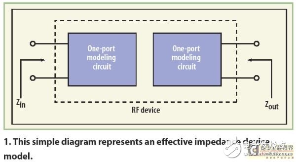
Due to the nonlinear nature of RF power transistors, a complete two-port device model is not an excellent choice for designing input and output matching networks. In this paper, a single port impedance model is employed to characterize the optimized load and source termination of the power device. In the RF device data sheet, the optimized load and the large source impedance 8 are typically given at several frequencies within the operating band of the RF power transistor. The effective input and output impedance of an RF device can be expressed as a conjugate change of these optimized terminations.
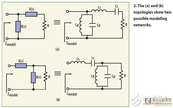
The RF power transistor characteristics can be characterized by measuring the optimized load and source impedance of the device over the entire relevant frequency band by means of a load-pull tuner. As shown in Figure 1, it requires a single port representation to predict complex conjugate changes in impedance from the low band end (FL) to the high band end (fH). In this example, Zout = Z*OL , Zin = Z*s; where ZOL is the optimized load impedance and Zs is the source load impedance. Figure 2 shows two possible topologies for the modeled impedance network. All losses are concentrated on one resistor that terminates an inductive-capacitor (LC) two-port network.
An analytical synthesis program can be used to implement a single-port network that matches the impedance data tested at both high and low frequencies. However, this tedious work can be replaced by analog software such as Touchstone (now ADS) to optimize the circuit elements of the modeling network to predict performance over the full band.
If the transistors are conjugated over a wide frequency range, as the frequency increases, the maximum gain that can be obtained will roll off at a negative slope of 6 dB/octave. One technique for compensating for the power gain variation of a transistor as a function of frequency is to selectively reflect some of the power at the lower end of the relatively high power gain band. However, the controlled loss of the technology leads to a weakening of the voltage standing wave ratio (VSWR) of the low-band input. The approximate power gain of an RF transistor is given by:

Where: fmax = maximum oscillation frequency; γ = a constant related to the change in gain, expressed by:

Where: x = slope in dB/octave. The matching network transmission loss caused by the input reflection is given by:

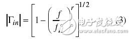
Where: Γin=reflection coefficient at the input.
In order to obtain a product with a constant Gα in the entire relevant frequency band,

Where: GH = gain of the high frequency side fH.
Using the optimization capabilities of Touchstone, an input matching network can be designed according to model equation 3.
The recommended broadband C-class PA computer design method can be summarized as the following system steps:
1. To get the required output power, gain, and supply voltage, select the large signal input and output impedance (Zin and Z*OL) from the device data sheet in the required frequency band.
2. Impedance data sampling points are extended using numerical interpolation and extrapolation techniques. This is a useful technique when determining the termination impedance of the device at frequencies fL, fo, and fH.
3. The terminal impedance is modeled over the entire frequency band using a suitable single-port network topology and its feature values ​​are optimized with Touchstone.
4. After designing the modeling circuit, an input and output matching network is inserted between the modeling circuit and the source and the 50 ohm load terminal. The initial evaluation of the elements of the matching network is done through a rough graphical design program.
5. The input and output matching networks are optimized to achieve the desired input and output matching. The output matching network is designed to achieve conjugate matching and to provide impedance ZOL to the transistor output over the entire frequency band. On the other hand, the input matching network is designed to achieve a flat gain between fL and fH. This can be achieved by selectively performing mismatches at lower frequencies. Bringing different sampling frequencies into Equation 3 estimates the input reflection coefficients and stores them in an external data file. The input matching network is then optimized to model the calculated input reflection coefficients over the entire frequency band.
6. Under the premise of maintaining the required frequency response, based on the actual situation, the elements of the matching network are modulated by the tuner window of Touchstone.
To verify the validity of the above program, a PA circuit was designed and built. The Class C PA has 10W output power from 225 to 400 MHz with a minimum power gain of 10dB. Because of the zero-biased emission-base structure, which is both efficient and simple in structure, Class C uses this structure. Due to its excellent reliability and durability, Motorola/Freescale's MRF321 UHF power transistor was selected. The MRF321 has 10W RF power at 400MHz and operates at 28V.
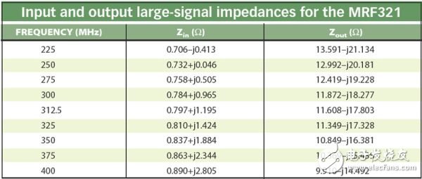
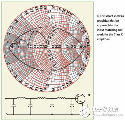
The design of the input and output matching network begins by selecting the input and output impedances (Zin and Z*OL) in the device data sheet and then inserting this data throughout the relevant frequency band (which can be done with Touchstone). The sample values ​​for these impedances inserted in the 225 MHz to 400 MHz band are shown in the table. Figure 4 shows the graphical design of the input matching network.
The input impedance of the center frequency (312.5 MHz) is at point A. The design goal is to not exceed the range specified by the constant Q when moving from point A to the center of the chart. among them:

Figure 4 shows that a low quality factor (Q) wideband matching network circuit can be implemented with multiple L sections. The matching circuit includes three low pass L-shaped portions and a bypass capacitor (C4) to compensate for the inductive reactance of the input impedance Zin.
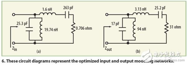
However, the network has a bandpass topology that includes two low-pass sections (L5–C5 and L6–C6) and one high-pass component (C7). The bypass inductor (L4) is used to neutralize the output capacitance of the transistor. Since the output impedance level is higher in this example, the gain-bandwidth constraint of the output matching circuit is simpler than the input matching circuit. The trapezoidal form of this network is useful in harmonic suppression.
The computer modeling program begins by designing a modeling network that predicts Zin and Zout from fL to fH. These networks are designed and optimized through Touchstone. Figure 6 shows the final optimized circuit element values ​​for these networks.
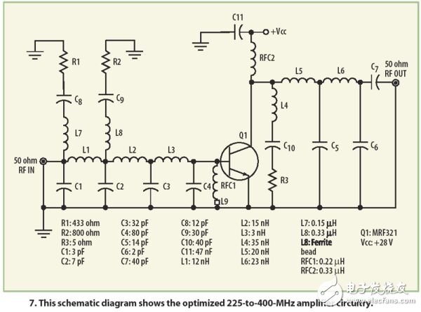
The input matching network is optimized to characterize the input reflection coefficient given by Equation 3 to compensate for the 6 dB/octave gain frequency slope of the MRF321 transistor. The author can request the Touchstone circuit file needed to optimize the input matching network. These required input reflection coefficient values ​​are saved as an external file (GMRF321.S1P). To control the input VSWR of the entire frequency band, two compensation networks consisting of L7, C8 and R1 and L8, C9 and R2 are added. On the other hand, the output matching network is optimized to provide an optimized load impedance ZOL for the transistor collector over the entire operating frequency band. A compensation network serialized with L4 has been added to improve the matching requirements. Figure 7 shows the final optimized power amplifier circuit.
The correct construction of the power amplifier begins with the correct selection of components for the matching network. All components are measured and tuned using Agilent's HP 8510B vector network analyzer. In addition to the ceramic fixed potentiometer, a trimmer capacitor is used for adjustment. All inductors are hand-wound from 20 and 22 AWG paint lines. An RF choke for an insulated DC circuit is made of a low Q type.
The circuit was fabricated on a 10.8 & TImes; 8 cm double-sided PCB using a 1.2 mm thick epoxy glass PCB material.
Epoxy glass is chosen because it can be bought anywhere and is cheap. The circuit is on top and the copper-clad bottom layer is grounded. For good circuit stability, a ferromagnetic bead is connected in series with the base choke to suppress low frequency oscillations. The circuit was then mounted in an 11&TImes;9&TImes; 3 cm housing to insulate the power amplifier from external interference signals. The housing is secured to a suitable heat sink. BNC connectors are used at the input and output for signal transmission. A feed-through capacitor is attached to the housing for DC biasing. The underside of the RF transistor is secured to the heat sink with a suitable screw. Figure 8 shows the output power as a function of frequency from 225 to 400 MHz.
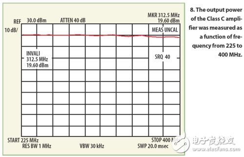
The power gain is 9.5 ± 1 dB. However, no attempt has been made to adjust the experience. Adjust the trimmer capacitor to have the same peak gain at both the high and low frequencies for better broadband operation. If so, a three-port circulator should be placed at the input of the power amplifier to protect the input power amplifier from the reflected power that may be generated by VSWR attenuation during the process. In the operating band, the second harmonic level is found to be 16 to 20 dB lower than the basic signal power.
Waterproof RGB LED Dance acrylic Floor Display Screen for Wedding Party
These interactive display walls are applied in different purposes. This is a perfect audio/visual solution for commercial or
business purposes as well as for the educational purposes. It is often used for providing information to the viewers or audiences in the most interactive and effective way .
prospective customers. The interactive LED can be used IN retail stores, restaurants and other commercial spaces for giving information about their services and products.
1.Aluminum Structure Light Weight,good heat dissipation, good weather resistance, convenient transportation.
2.Imported PC Protrctive Surface, High Permeability, Strong Impact Resistance, Good anti-slip Effect
3.Strong Load Capacity The center of the panel has a load-bearing pivot,with a single panel bearing more then 1.2tons
Dance LED Display,Flexible Led Screen,Indoor Led Display Screen,Led Church Screen
Guangzhou Chengwen Photoelectric Technology co.,ltd , http://www.cwstagelight.com