TI's TPS65580 is an advanced three-terminal output D-CAP2 mode synchronous buck converter chip that enables system designers to provide cost-effective, low-cost devices when providing power regulators for a wide range of end devices Low standby current solution. The TPS65580 chip master loop uses D-CAP2 mode control to provide efficient and fast transient response without external compensation.
The TPS65580 is suitable for low equivalent series resistance (ESR) output capacitors such as POSCAP or SP-CAP, as well as ultra low ESR ceramic capacitors. The device provides convenient and fast operation with an input voltage of 4.5V~18V.
The TPS65580 is available in a 4.4mm & TImes; 6.5mm 20-pin TSSOP (PWP) with an operating temperature range of -40°C to 85°C.
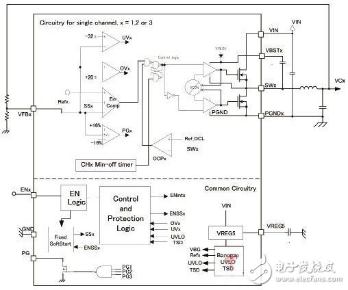
Figure 1 TPS65580 internal block diagram
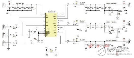
Figure 2 Schematic diagram of the TPS65580 scheme
TPS65580 main features
• Advanced D-CAP2 control mode
• Fast transient response
• Loop compensation eliminates the need for external parts
• Compatible with ceramic output capacitors
• Wide input voltage range: 4.5V~18V
• Output voltage range: 0.76V~7.0V
• Efficiently integrated FET optimized low duty cycle applications
• 160MΩ (high voltage side) and 130MΩ (low end) at 2.5A
• 250MΩ (high voltage side) and 230mΩ (low end) at 1.5A
• High initial reference accuracy
Table 1 TPS65580 program material list
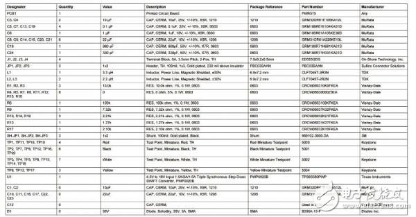
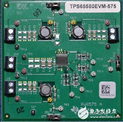
Figure 3 PCB component layout (1)
• Low side RDS (on) lossless current sensing
• Fixed 1.2ms soft start
• No outflow pre-bias soft start
• 700kHz switching frequency
• Cycle-by-cycle overcurrent limit control
• OCL, OVP, UVP, UVLO, TSD protection
• Snoring timer overload protection
• Good power supply
• Integrated boost PMOS adaptive gate driver switch
• OCP constant, thermal compensation RDS (ON) (4000ppm / °)
• 20-pin HTSSOP
TPS65580 application
• Low power system load point adjustment for a wide range of applications
• Digital TV power supply
• Network home terminal
• Digital Set Top Box (STB)
•DVD player/recorder
• Game consoles and other
TPS65580 solution
Texas Instruments' TPS65580EVM-575 Evaluation Module (EVM) is a fully assembled and tested circuit for evaluating the TPS65580 synchronous buck converter. The EVM includes an input-output synchronous buck converter rated at 12 V with three output channels. Output channel 1 is 3.3V, 1.5A, channel 2 is 1.2V, 2.0A, and channel 3 is 1.5V, 1.5A. Its input voltage range is 4.5V~18V. TPS65580 can control each output channel and a good combination Power function. The TPS65580 features DCAP2 control with a pseudo fixed switching frequency of 700kHz for fast transient response (smaller output capacitance).
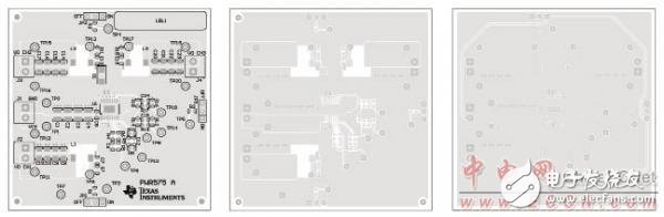
Figure 4 PCB component layout (2)
TPS65580 reference program features
• Synchronous Buck Converter
• 3 outputs
• Internal slow start
• Wide input voltage up to 18V
• Integrated FET
Xinxiang Mina Import & Export Co., Ltd. , https://www.mina-motor.cn