Electron microscopy is transitioning from the lab to industrial applications, with a strong emphasis on speed and user-friendliness. The first intelligent, high-speed imaging scanning electron microscope was introduced in Beijing, marking a significant step forward. Not only does it support scientific research, but it also enhances engineering applications, opening new pathways for exploring the microscopic world.
This paper outlines how the domestic high-throughput scanning electron microscope (HT-SEM) has been tailored for industrial use, continuously evolving to meet practical demands. It covers five key areas: functional performance, core components, independent design, operation, manufacturing, and maintenance. By focusing on the first-generation concept and structure of the next generation, it provides a comprehensive solution and application platform to achieve advanced performance goals.
First, performance optimization and upgrades have been a central focus. While laboratories prioritize detailed experimental results, industrial production emphasizes speed and efficiency. High throughput is therefore the top priority. Measured by pixels imaged per second, traditional SEMs typically operate at tens of megapixels per second. However, the domestic industrial SEM has surpassed 100 MPixels/s, setting a new benchmark. Both secondary electron (SE) and backscattered electron (BSE) channels can reach up to 200 MPixels/s, enabling the capture of 200 high-motion images every second—like turning a camera into a dynamic video recorder. This advancement transforms high-throughput SEMs from static observation tools into powerful devices for capturing real-time changes.
The breakthrough in achieving such high throughput comes from Qualcomm’s big data acquisition technology, supported by a unique electronic optical structure and system design. This ensures rapid acquisition of sample information, with imaging speeds nearly 100 times faster than conventional SEMs.
Figure 1 shows the appearance of the high-throughput industrial scanning electron microscope.
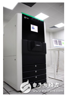
**Figure 1. Appearance of the high-throughput industrial scanning electron microscope**
Second, device updates are ongoing. Figure 2 illustrates the internal structure and main components of the industrial scanning electron microscope. To achieve high throughput, all key parts—from the lens barrel to the sample stage—have been redesigned with advanced materials and integrated systems. The update cycle continues to shorten.
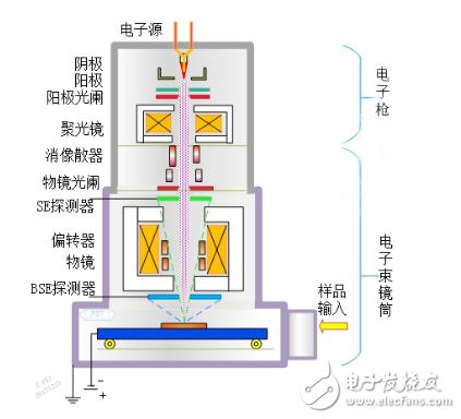
**Figure 2. Schematic diagram of the internal structure of the domestic industrial scanning electron microscope**
The design of the barrel has evolved from a traditional "tall" shape to a more compact, slim form. It is installed inside a cabinet without the need for knobs, allowing users to operate directly via a touchscreen and computer interface.
The electron source is the first critical component. The electron gun uses a Schottky thermal field emission, producing a large beam with a nanometer-level fine tip to enhance emission efficiency.
The new generation of objective lenses plays a crucial role in the domestic industrial SEM. Historically, objective lenses have gone through several generations, including MOL, SOL, BOL, VOIL, SOIL, and SORIL. These represent different structural approaches aimed at improving resolution and field of view. Today, the high-resolution large-field objective system features a new composite deflection acquisition design.
The decelerating electrostatic lens helps collect electronic signals, increasing the collection of SE and BSE for better resolution. For non-conductive biological samples, this prevents charge buildup, which could otherwise distort image quality. By slowing down the electrons between the objective lens and the sample, the beam remains at low energy, reducing the risk of charging and ensuring clearer images.
The new composite deflection acquisition system integrates advanced signal collection methods. Innovative detectors have become essential components. From traditional scintillator + PMT setups, the system has evolved to coaxial semiconductor detectors with gain amplifier circuits, significantly improving electron collection efficiency.
High-resolution imaging over a large field of view meets the needs of observing both material and biological samples. Theoretical calculations and practical tests confirm that even when scanning large areas, edge aberrations remain minimal, allowing clear focusing and expanding the visible range. This makes the high-throughput SEM an invaluable tool for modern industrial and scientific applications.
Laser radar contains LSPD safety laser scanner and LS laser radar. LSPD safety laser scanner is type 3 with CE certificate. It can be used for agv safety and industrial area protection. LS laser radar is for agv guide. Many famous agv manufacturers has installed LS laser radar to guide their agvs. Feedback from customers are quite posotive.
Laser Radar,Auto Guided Vehicle Guide Radar, Laser Radar,Safety Scanner,Safety Laser Scanner, Laser Radar
Jining Keli Photoelectronic Industrial Co.,Ltd , https://www.sdkelien.com