1. DRFM Data Acquisition Module Design
1.1 Main Features of MAX101A
The ADC chip is the core component of the data acquisition system. The A/D converter used in this system is the MAX101A from Maxim, which offers a maximum sampling rate of 500 Msps and an 8-bit resolution. To achieve a higher sampling rate of 1 Gsps, two MAX101A chips are used alternately. Key features of the MAX101A include:
- Conversion rate up to 500 MHz;
- Effective number of bits (ENOB) of 7.0 at 250 MHz;
- Analog input bandwidth of 1.2 GHz;
- Integral non-linearity (INL) error less than ±1/2 LSB;
- Supports both differential and single-ended inputs with 50 Ω impedance;
- Input voltage range of ±250 mV;
- Data path supports dual latch output.
An image illustrating the front-end design of the data acquisition system based on DRFM is shown below:
1.2 Working Principle of MAX101A
(1) Multi-Bit Conversion
The MAX101A uses a parallel architecture, also known as a flicker structure, enabling faster multi-bit conversion compared to traditional ADCs. It contains 255 comparators when operating at 8-bit resolution, each responsible for detecting one least significant bit (LSB). These comparators are divided into two sets, A and B, and their outputs are latched on alternate negative edges of the input clock signal.
(2) Track/Hold Function
The internal track/hold amplifier enhances the accuracy of valid data bits, especially at high slew rates. This circuit reduces the input voltage by a factor of 4, making it compatible with a ±1.02 V reference. It also provides a differential 50 Ω input, simplifying the interface with the ADC.
(3) Data Flow
The track/hold amplifier captures the analog input voltage and splits it into two parts, working on alternate negative edges of the input clock. The DCLK output is derived from CLK and is either divided by 2 or 10, depending on the configuration. This allows precise timing control for the data output.
1.3 Applications of MAX101A
(1) Analog Input Range
Although the normal operating range is ±250 mV, the actual input range is ±500 mV relative to ground. This allows for a wider dynamic range, accommodating both AC and DC components in the signal. For full-scale output, a differential input of +250 mV is required between AIN+ and AIN-.
(2) Reference Voltage
The reference resistor string is driven by an internal buffer amplifier. Adding an RC network to the reference input improves noise performance. A 33 Ω resistor and a 0.47 μF capacitor should be placed close to the MAX101A package to minimize noise effects on the ADC's performance.
(3) Clock Signals (CLK and DCLK)
All clocks are differential. The CLK and DCLK signals are internally synchronized through a 50 Ω resistor. Only one pair of CLK and DCLK inputs is active, while the other is grounded via a 50 Ω transmission line. DCLK controls the timing of data outputs, and its frequency is typically half that of CLK.
(4) Output Mode Control (DIV10)
When the DIV10 pin is grounded, the device operates in detection mode, dividing the input clock by 10. This reduces the output data rate but maintains a 50% duty cycle. If the pin is left floating, the device operates in normal mode.
(5) Power Supply and Grounding
The MAX101A requires a +5V and -5.2V power supply. Decoupling capacitors (0.1μF and 0.01μF ceramic) should be placed close to the power pins. All ground pins must be connected to a ground plane to reduce noise and improve accuracy.
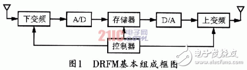
2. Data Cache Module Design
The data buffer in this system uses Altera’s FLEX10KE series CPLD. This design leverages high-speed FIFOs for efficient data buffering. Since the input and output clock frequencies differ, a dual-clock FIFO is necessary. The low-voltage operation of these devices significantly reduces power consumption and increases system flexibility and reliability.
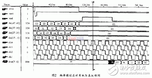
The system is programmed using VHDL in the MAX+PLUS II v9.6 environment. A modular design approach was adopted, including four main modules: FIFO, MUX, counter1, and counter2. The FIFO can either use the built-in LPM_FIFO macro or be manually implemented. In this case, the macro was used due to its efficiency and ease of configuration.
The MUX and counters are custom-designed and integrated into the system module. Once all sub-modules are completed, a top-level system module is created to define the overall logic and connections. This approach makes future modifications easier. A simulation waveform of the system is shown below:
3. Conclusion
This paper focuses on the design of the DRFM data acquisition front end. In ultra-high-speed data acquisition systems, achieving sampling rates of hundreds of megahertz or even 1 GHz remains a challenge, both domestically and internationally. Using SRAM-based CPLDs instead of high-speed FIFOs helps reduce power consumption and system complexity. Implementing the data cache on a single chip not only simplifies hardware but also lowers power requirements.
Moreover, CPLDs offer reconfigurability through programming, allowing for easy updates and improvements to the system. This flexibility makes them ideal for future enhancements and ensures the system remains adaptable to evolving requirements.
ELFWORLD MC8500 Disposable Vapes
ELFWORLD MC8500 Disposable Vape is pre-loaded with 16ml vape juice at strength, running on a rechargeable 650mAh battery, you can enjoy second-to-none vapor via its integrated mesh coil, and each device delivers up to 8500 puffs. Its elongated C-frame design, adorned with a stylish faux resin exterior, adds a touch of elegance, and the inclusion of a lanyard enhances portability and convenience. The mesh coil ensures optimal flavor and vapor production for as many as 8500 puffs.
Disposable Vape, E cigarette, Eshisha
Shenzhen Yingyuan Technology Co.,ltd , https://www.yingyuanvape.com