Introduction
In many harsh environmental systems, a growing trend is that high-precision electronic devices are getting closer and closer to high-temperature areas. Behind this trend are several driving factors that are reflected in energy exploration, aerospace, automotive, heavy industry, and other end-use applications. 1 For example, in the field of energy exploration, the ambient temperature increase is a function of the depth, and the typical operating temperature of related equipment is 175°C and above. Due to size and power limitations, active cooling is not practical and thermal convection is very limited. In other systems, sensors and signal conditioning nodes need to be placed near high temperature areas, such as engines, braking systems, or high-power energy conversion electronics to increase overall system reliability or reduce costs.
Historically, it is difficult for engineers to design reliable high-performance electronics for these applications because the market lacks manufacturers to produce specified components for these operating conditions. Fortunately, more and more (IC and passive) components have emerged in recent years, and manufacturers specify operating temperatures as high as 175°C and above. In addition, the recent reference design also focuses on performance, combining some of these components in the signal chain subsystem to achieve precise data acquisition, so that system designers can quickly adopt related technologies (such as CN-0365) and help them Reduce design risk and shorten time to market. However, before this, there were still some gaps in high-temperature precision data collection, and full-featured, widely available, full-featured platforms.
In this article, we will introduce a new high-temperature precision data acquisition and processing platform with a working temperature of up to 200°C. The platform includes a high-temperature circuit assembly, as well as a data acquisition front-end and microcontroller, optimized firmware, data acquisition and analysis software, source code, design files, bill of materials, and test reports. The platform is suitable for reference design, rapid prototyping and laboratory testing of high-temperature instrumentation systems. The size and structure of the circuit components have been specifically designed to be compatible with the size requirements of oil and gas instrumentation, but they can also be used as the basis for other high-temperature applications.
Hardware Architecture Overview
Instrumentation used in oil and gas exploration (also known as downhole tools) is similar to many sophisticated data acquisition and control platforms, but has specific requirements for performance and reliability and can be used as a case study for this reference platform. In this application, the system samples the signals from various sensors to collect information related to the surrounding geological structure. These sensors may be electrodes, coils, piezoelectric sensors, or other sensors. Accelerometers, magnetometers, and gyroscopes can provide information about the drill string's pitch and speed. Some of these sensors have very low bandwidth requirements, while other sensors provide information at or above the audio frequency range. Multiple acquisition channels are required and high precision must be maintained at high temperatures (typically 175°C and above). In addition, a large part of these instruments and meters are battery-powered or have limited available power. Therefore, they must have low power consumption and multiple operating modes in order to optimize power consumption.
In addition to the requirements related to electronic systems, there are mechanical limitations in downhole applications that may determine the size of electronic components and may also affect the assembly and selection of components. For the latter problem, we will discuss in detail in the following sections. At present, it should be noted that the circuit components in this section generally have a limitation on the width of the circuit board. The electronic component must be placed in a tubular pressure vessel used in drilling operations, so its aspect ratio is narrow and long. This shape feature limits the size and density of the available components, and may also limit the layout of the component layout and signal routing. As a result, it may affect the performance of high-precision electronic devices. Therefore, special attention must be paid to layout and other package design details. . Figure 2 shows a circuit pack (transparent, top) in a typical size, mounted in a tubular pressure vessel, with a cross-section (bottom) of the tubular pressure vessel after the circuit board is installed. The reliable reference design platform discussed in this article is based on the CN-0365 analog front end reference design. Its purpose is to lay the foundation for high-precision low-power microcontroller-based precision data acquisition and control solutions to meet a number of downhole instrumentation and other high-temperature electronics. Device requirements. Based on the AD7981 analog-to-digital SAR converter, this reference design presents a fully functional system with two high-speed synchronous sampling channels and eight additional multiplexed channels to meet the data acquisition requirements of a wide range of downhole tools. 10 channels). The analog front-end accesses the VA10800 ARM® Cortex®-M0 from alliance partners Vorago Technologies and Petromar Technologies through the SPI port. This design is the latest addition to the growing ecosystem of ADI's high temperature applications and solutions.
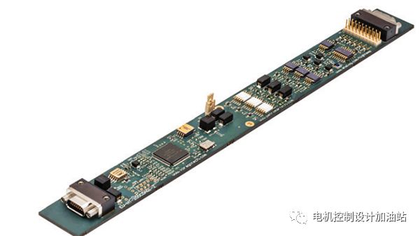
Figure 1. High temperature reference platform.
After the acquisition, the data can be processed locally or transmitted via the UART or optional RS-485 communication interface. Other complementary components on the circuit board (including memory, clock, power supply and passive components) are specified by their respective suppliers and support high operating temperature components. These components have been verified to be reliable at temperatures of 200°C and above. Work. Figure 1 and Figure 2 show the actual circuit board diagram and high-level functional block diagram of the high-temperature reference platform. The circuit board shown in Figure 2 shows the layout and dimensions of the downhole circuit board, measuring approximately 11.4 inches long and 1.1 inches wide.
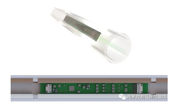
Figure 2. Downhole electronics size.
The CN-0365 application note comprehensively describes the design issues of the platform's precision data acquisition channels. The design is the basis for the three ADC inputs on this platform, but to meet the board size requirements, the platform is capable of reliable operation at temperatures up to 200°C, with some adjustments in the selection of passive components and optimization. Reference acquisition channel circuit shown in Figure 4. There are two digital multiplex channels that can operate at high sample rates, each containing a complete data acquisition channel (similar to the CN-0365). There is also an analog multiplex channel that adds an ADG798 multiplexer before the input and is optimized for low-throughput inputs. R1 and R3 provide a 1.25 V bias voltage for U1's non-inverting input to prevent it from floating to the analog input supply rail when it is disconnected or when the multiplexer is deselected. You can change R8 and R9 to increase the gain of U1. R4, R7, and C1 are antialiasing filters, but they can also be reconfigured as attenuators or alternate filter configurations. R5, R6, and C4 form an RC filter between the ADC driver and the ADC input. This filter limits the amount of out-of-band noise reaching the ADC input and attenuates the kickback voltage from the ADC's input switching capacitor.
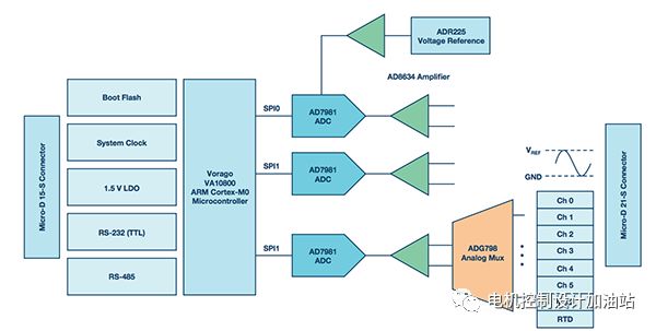
Figure 3. High-temperature reference platform functional block diagram.
This platform was designed to take advantage of several key features of the AD7981 ADC. This 16-bit, 600 kSPS converter provides a typical SINAD of more than 85 dB and a typical INL of ±0.6 LSB, with a 2.5V reference and no missing codes. With a 5 V reference, more than 90 dB of SINAD can be achieved, but in this platform, we did not choose this specification in order to maintain compatibility with lower voltage systems. Since the ADC core automatically enters a power-saving state between conversion cycles, the power consumption of the ADC changes linearly with throughput. This saves energy when using a low sample rate converter.

Figure 4. ADC driver configuration.
Software Overview
firmware
The platform's firmware is based on the FreeRTOS operating system, making it easy to integrate tasks such as data processing and other communications. We optimized the code so that non-multiplexed channels 0 and 1 can perform fast ADC conversion efficiently, and the conversion of multiplexed channels 2 to 9 takes as little as 10 μs. The conversion result can be processed locally or at 2 Mbps from the UART channel. The size of the conversion result buffer is 16 kB (result of 8 k samples), which can be shared between multiple channels or used exclusively for one channel. The firmware is provided in an open source format that can be customized by the end user and used as the basis for the final application.
Data Acquisition and Analysis Software
Figure 5 shows the data acquisition and analysis software. Based on the .NET interface design, the power components pass a USB UART-TTL level shifter. With well-defined protocols, you can communicate with hardware, including control and data flow. Data can be collected in burst mode or continuously. In addition, data analysis functions are included to analyze and verify SNR, THD, and SINAD (such as FFT) in the time domain and frequency domain. Data can also be recorded to a file (eg exported to Excel) for storage or processing in other applications. Just like the firmware, we provide the source code of the data acquisition software for free, and the end user can customize it.
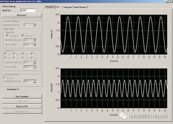
Figure 5. Data acquisition and analysis software.
High temperature structure
This reference platform is made of components and other materials suitable for operation at 200°C. All components used on the platform are high-temperature components specified by their respective manufacturers (unless otherwise specified), and a large network of distributors worldwide has already begun to supply them. All BOM, PCB layout drawings and assembly drawings are provided free of charge with the reference design package.
capacitance
Use C0G or NP0 dielectric capacitors for small-value filter and decoupling. The temperature coefficient of these dielectric capacitors is extremely flat, and in general, they are more resistant to buckling stress.
In order for the RC filter to have a high Q, low temperature coefficient, and stable electrical characteristics at varying voltages, it is recommended to use C0G or NP0 type capacitors. We use small-size 0805 or more ceramic devices to reduce the CTE mismatch between the component and the PCB. For large storage needs, we chose a high-temperature tantalum capacitor and made a balance between size and ESR.
resistance
The main part of the design uses thin-film SMT resistors (automotive-grade PATT series), and there are sufficient sources on the market. In addition, a portion of the thick film SMT resistor was selected for the specific value and size according to design requirements.
Connector
The board is connected to a Micro-D rated at 200°C, which is often used in high-reliability industries. In order to reduce signal crosstalk, we specially deal with the connector housing and ground it to the PCB in the assembly. For applications that require the highest signal integrity and minimum crosstalk, high-temperature professional connectors (or no connectors) and coaxial or shielded balanced inputs are used to reduce crosstalk.
PCB design and layout
It is advisable to choose a narrow PCB for downhole applications because the circuit board in these applications must meet the drilling and pressure shell restrictions. The circuit board material chosen is a high temperature, halogen-free polyimide. Specify a board thickness of 0.093 inches instead of the standard thickness of 0.062 inches as this will increase stiffness and flatness. Nickel gold surface treatment, in which nickel provides a barrier to prevent intermetallic proliferation, gold provides a good surface for joint welding.
For a selected board thickness of 0.093 inches, a typical four-layer stack has a copper isolation layer of about 13 mils and a large core of 60 mils. If it is a six-layer structure, the isolation layer is generally 9.5 mils thick and 28 mils thick. For this reason, we have adopted a six-layer design so that a ground plane can be provided at each signal layer to improve noise performance. Power and digital communication signals are fed into one connector and analog signals are fed into the reverse connector. This allows good isolation and signal flow between the digital domain and the analog domain. The division of the ground is located in the middle of the circuit board, and the power supply filtering is located near the partition. Minimize the number of digital control lines that intersect the separation layer and use series termination to reduce digital noise coupling. Solder the digital and analog ground planes at one point using a copper network connection to provide a low-impedance circuit for the drive source.
The multiplexer control signal has the same length as the analog section, but its routing path is separated from the critical analog signal path. In practice, these multiplexed control lines can be changed synchronously with the acquisition data measurements, thereby minimizing crosstalk effects. The solder selection Sn95/Sb05 is designed to provide a sufficiently high melting point (>230°C) at an operating temperature of 200°C, while also taking into account good operability and the existing processing capabilities of the assembly plant.
Circuit board installation
We provide mounting posts on this board for ease of consideration. They are only suitable for benchmarking or laboratory environments and are not suitable for strong impact and strong vibration environments. If you want to use in strong impact and strong vibration environment, you can use epoxy resin to fix the component on the circuit board. Fragile components such as IDC connectors can be sealed or removed from the assembly. In downhole or other harsh environments, the typical installation method is to use a rail mounting system, the entire circuit board is fixed with a flexible impact mounting washer. It is also possible to completely seal the assembly and install it in the mounting hardware, and then fix the mounting hardware to the chassis or housing. For more information on related devices, see the article "Low-Power Data Acquisition Solutions for High-Temperature Electronics Applications."
Performance test results
We have extensively tested a number of boards to assess their typical performance over the operating temperature range; and also soaked at 200°C ambient temperature for 200 hours to determine assembly process and board reliability.
The AC and DC signal chain performance is a key precision indicator based on the SAR ADC's precision data acquisition system. When the ADC operates at 600 kSPS and the operating temperature is 200°C, the robust ratiometric platform can achieve crosstalk performance of more than –100 dB with a maximum offset drift of ±60 mV. For AC testing, use a low-distortion 1 kHz tone as the input signal and power the board with +5 VDC/–2.5 VDC analog power. Figure 6 shows the FFT and spectrum analysis results of the tone at 400 kSPS. At 200°C, the SNR is better than 84 dB with a THD of –96 dB. Figure 7 shows the SNR and SINAD. Figure 8 shows the THD of the non-multiplexed channel over the operating temperature range when using the same input tone.
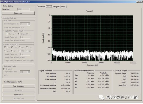
Figure 6. FFT and spectrum analysis results at 200 °C.

Figure 7. SNR and SINAD over the operating temperature range.
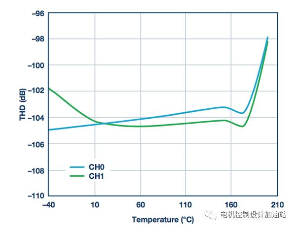
Figure 8. THD over the operating temperature range.
We measured the power consumption of the analog and digital rails over the operating temperature range. The results are shown in Figure 9. The total power consumption at room temperature is 155 mW, which is increased to 225 mW at 200°C. Power consumption on the 3.3 V rail is dominated by a microcontroller operating at full clock speed and a precision oscillator. We set the burst sampling rate for the converter to 8192 samples per second.
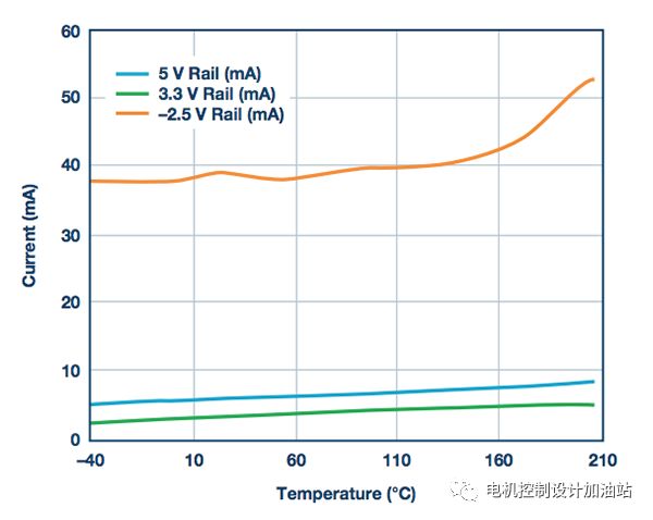
Figure 9. Power Dissipation for 2.5 V, 3 V, and 5 V Supply Rails
For test results of additional parameters, see Reference Platform, whose rated parameter specification meets the 200°C operating temperature requirement.
Application example
Many applications in the fields of oil and gas exploration, aerospace and heavy industry achieve orientation and vibration detection through accelerometers. Accelerometers with analog inputs have the highest accuracy and are flexible enough to adjust the sensor output according to the needs of the application.
The ADXL206 is a complete precision low power dual-axis iMEMS® accelerometer for use in high temperature environments. It has a range of ±5 g and a bandwidth of 0.5 Hz to 2.5 kHz. The output of the ADXL206 is centered on 1â„2 VCC, which is proportional to VCC. If the ADXL206 and the EV-HT-200CDAQ1 share VCC (available on the connector), the dc offset and power supply drift can be cleared with the VCC reference on the multiplexer S7 channel. Figure 10 shows an example circuit. The ADXL206 signal range (0 V to 5 V) must be scaled by a 1â„2 scaling factor to fit the precision data acquisition system's 0 V to 2.5 V range. The specific method is to buffer the output first and then use the attenuator inside the data acquisition system. C2 and C3 set the bandwidth of the ADXL206; the bandwidth shown in the example in Figure 9 is 33 Hz. Low-bandwidth applications can use multiplexer inputs; to achieve the highest bandwidth and accuracy, two non-multiplexed input channels can be used.

Figure 10. High-temperature accelerometer interface with the EV-HT-200CDAQ1.
summary
This article introduces a new, highly integrated, robust, precision data acquisition reference platform, the EV-HT-200CDAQ1. The platform has been tested and its specifications meet the 200°C operating temperature requirement. With this platform, high-electronic system designers can use the most advanced components in prototyping and evaluation, thereby reducing development time and time-to-market. For more information on this platform, including the entire design package and software, click here.
Data Cable,Fast Data Cable,Data Power Cable,Data Transfer Cable
Guangzhou YISON Electron Technology Co., Limited , https://www.yisonearphone.com