The role of the power monitor is to control the system's point of load (POL) so that the power rail meets regulatory requirements. POL can be analog or digital depending on the type of output signal. This article describes how to implement a basic implementation of power monitoring using SoCs. To better illustrate the key implementation principles, we take the application of the Cypress On-Chip Programmable System (PSoC) as an example. PSoC works in conjunction with analog/digital POL. The main features of the power monitor include the following:
1, enable the regulator / power supply
2. Monitor the voltage or current of the power rail
3, adjust (trim) power supply current
4, fault handling and recording
5, host communication
The block diagram of the entire system contains the following functions as shown in FIG.

Figure 1. Power Monitor System
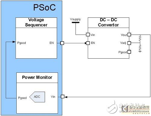
Let's take a look at the simplest power monitoring architecture and build on it to understand the entire system. In the simplest power monitoring architecture, the microcontroller is responsible for monitoring the Power-Good (PGood) output and deciding whether the DC-DC converter should be enabled or disabled. The microcontroller can monitor multiple outputs and properly enable (power-up) or disable (power-down) the converters in sequence. This function is performed by the Voltage Sequencer (VS) component in PSoC. Located inside the PSoC Creator IDE, this component groups hardware and firmware for specific functions. The PSoC component has been mentioned many times in this article and can be considered a "virtual chip" in a large chip.
Figure 1 shows the basic power monitoring structure with only voltage sequencing, which is provided by most microcontrollers. Voltage sequencing also includes more functions such as power rails based on multiple prerequisites and precise timing. To achieve these higher levels of functionality, additional design is required for timing analysis. For ease of understanding, the example in Figure 2 shows only one power rail. It should be noted that each board in the current system may require more than 20 power rails. Each SoC chip can support up to 32 power rails, more than three times the current dedicated power monitoring architecture of the Specialty Standard Products (ASSP).

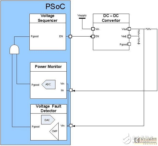
Figure 2. Power rail enable and sequencing Most designers do not want to rely solely on a simple DC-DC converter PGood signal with a hard-coded threshold. Therefore, it is usually necessary to control the enable pin of the DC-DC converter according to the voltage and/or current conditions of different power rails. This requires the use of an ADC and associated logic to control the enable pin. To do this, we use a power monitor (PM) component to monitor the voltage and current of different lines and provide a status output for each line. These status lines are connected to a voltage sequencer that controls the enable signal. The block diagram of the design is shown in Figure 3, which contains the power monitor. SoCs with accurate ADCs and the ability to use digital logic can do this. The ADC can be used to capture the voltage value and then generate a PGood signal based on a pre-set voltage level in the firmware.
The current monitoring can be realized by using a microcontroller that supports current measurement, and the current value can be derived by using a shunt resistor and measuring the resistance voltage, thereby implementing current monitoring. For PSoC devices, the current measurement actually measures the voltage across the shunt resistor, and the accuracy of the PM voltage and current measurements is 0.26%. Since the voltage output has been measured by the PM, the current measurement only needs to add one pin. These pins are called current measurement pins.

Figure 3. Power Monitoring and Voltage Sequencer
Power monitors with ADC and firmware provide a number of advanced features such as recording voltage and current values ​​in the EEPROM at the time of the fault. However, implementing these features can cause CPU latency and require attention in mission-critical applications. To solve this problem, a complete hardware voltage fault detection (VFD) component can be implemented using hardware modules such as comparators and DACs. A voltage digital-to-analog converter (VDAC) can be used to set the overvoltage (OV) and undervoltage (UV) thresholds in the hardware. If the SoC has multiple DACs that support hardware fault detection, each power rail can be set up with dedicated hardware. In a programmable microcontroller such as PSoC, the same hardware can be configured to perform this function by direct memory access (DMA) components and setting the DAC and comparator with the required connections and parameter values.
The Pgood signal of the hardware fault detector and the power monitor can be integrated to obtain the Pgood signal of the voltage sequencer, as shown in Figure 4.

Figure 4. Add hardware fault detection
All modules discussed so far can be turned on or turned off when the required voltage or current is deviated. In some cases (such as commissioning or adjustments to new requirements), the voltage output of the DC-DC converter needs to be adjusted to a new level. This feature is called trimming or fine tuning (TM) of the power rail. The trimming function is mainly used for systems that require field adjustment after production. This feature may need to be used in real time after the product is manufactured. The fine-tuning function is used to test the system itself during development or before production. This feature can be used to test, characterize or verify system performance at different voltage limits.
To achieve these functions, the Vadj (voltage regulation or voltage feedback) of the DC-DC converter should be raised or lowered as required. The power monitor is responsible for measuring the current voltage value, while the trimming or trimming circuit is responsible for adjusting the new voltage value. The PWM-DAC can be used to trim the voltage output, such as using a low-pass RC circuit (external) to filter the PWM output. If we want Vout to be lower than its current value, we can increase the PWM duty cycle to increase the Vadj value. This causes the DC-DC converter to reduce its output voltage Vout according to its Vadj pin voltage. This function can be implemented either with the DAC (if any) or with the PMW and adding an external RC filter, as shown in Figure 5. The accuracy achieved by implementing this function with a PWM-DAC is 0.60%.

Figure 5. Add trimming and fine-tuning to store system-detected faults in non-volatile memory for ease of use. In this example, the EEPROM is used to store all the fault records, and the flash memory is used to save the user settings.
All of the data and settings discussed so far can be used or configured by the host device through different forms of communication. The most popular protocol in the field of power monitoring is the Power Supervisory Bus (PMBus) protocol. PMBus is a system management communication protocol built on the I2C communication interface. PMBus can be used to obtain information about the status of different power lines, the settings of the DC-DC converter, and many other detailed instructions pre-set by the protocol. Additional custom commands can be added to use additional commands other than the predefined PMBus protocol. PMBus can be used to read all state and component parameters and override any other component parameters. This allows customers to use any reprogramming technology to upgrade the system in real time. In this example, the PMBus protocol is built on top of the existing I2C module, as shown in Figure 6. In addition to the PMBus components, a complete power monitoring solution is available with a PMBus host emulator GUI to support system design and debug.

Figure 6. Adding PMBus communication to the power monitoring system
All modules are provided as components, as shown in Figure 7.

Figure 7. All modules are provided as components
This article describes the building blocks required to build a power monitor system. All or part of the modules should be selected depending on the final application. You can build your own power monitor system with the selected SoC and the modules mentioned in this article. Advanced features that can be implemented using SoC-based systems include temperature measurement, fan control, single-event up (SEU) processing, and bootloader.
Fiber Optic Ip68 Enclosure,Ftta Ip68 Hardened Connections Device,Ftta Ip68 Hardened Connections Fast,Fiber Optic Ip68 Enclosure Adapter
Huizhou Fibercan Industrial Co.Ltd , https://www.fibercannetworks.com