The frequency synthesizer is a crucial component in both the transmitting and receiving systems. It utilizes phase-negative feedback frequency control technology, offering excellent narrowband carrier tracking performance and bandwidth modulation tracking capabilities. Additionally, it provides local oscillator signals for phase up- and down-conversion, effectively suppressing phase noise and spurs. The frequency source implemented through phase-locked frequency synthesis technology has found widespread application in fields such as radar, communication, and electronic systems.
This paper discusses the design of a GPS signal source as a reference, with a focus on the typical application of Analog Devices’ frequency synthesizer, ADF4360-4, in GPS signal source development.
1 Signal Source System Composition 1.1 System DesignAccording to existing literature, the structure of GPS signals is well understood. The primary goal of designing a GPS signal source is to simulate the signals transmitted by satellites, specifically performing baseband modulation of GPS signals and generating an RF signal at 1,575.42 MHz. In the overall system design, a superheterodyne up-conversion approach is adopted. The system is divided into digital and analog sections. As shown in Figure 1, the digital part follows the software-defined radio concept, using a GPS chip to perform baseband and intermediate frequency (IF) modulation, outputting an 8-bit GPS digital IF signal. This signal is then converted to an analog signal via a D/A converter and sent to the analog section.
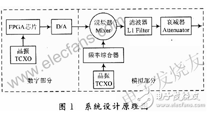
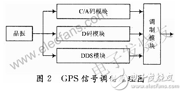
(1) Digital Circuit: The digital circuit module focuses on baseband/IF design and follows the software radio idea. Using a GPS chip, the system generates the GPS navigation message (D code), C/A code, and a digital IF carrier, performing baseband modulation. The spread spectrum modulation results in a 12.5 MHz GPS digital IF signal. The modulation process involves the C/A code module, D code module, DDS module, and a modulation module. The C/A code module generates a sequence of 1.023 MHz, lasting 1 ms, while the D code module produces a 50 Hz navigation message. The DDS module creates a 12.5 MHz digital carrier, and the modulation module performs BPSK and spread spectrum modulation on the signals.
(2) Analog Circuit: The analog circuit module is responsible for the RF circuit design. Components like the frequency synthesizer, mixer, filter, and attenuator are used to convert the IF signal to the RF domain. The signal is filtered and adjusted in power through an adjustable attenuator before being output as a GPS RF signal, completing the up-conversion function.
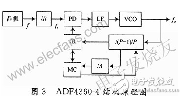
2 Frequency Synthesizer ADF4360-4 2.1 Working Principle and PerformanceThe main function of a frequency synthesizer is to provide a local oscillator signal for up-conversion. It is commonly used in transmitters and receivers, typically consisting of a digital phase detector (PD), loop filter (LF), voltage-controlled oscillator (VCO), and programmable counters (R and N counters). The PD compares the outputs of the R and N counters, generating an error voltage that is filtered by the LF and used to control the VCO, producing the desired frequency.
The ADF4360-4 is a high-performance phase-locked frequency synthesizer from Analog Devices. It operates in dual-mode pre-frequency division, allowing for improved frequency resolution without changing the output frequency range. Its output frequency ranges from 1450 to 1750 MHz, with two selectable modes, and can generate frequencies between 725 and 875 MHz when in the two-way mode. It operates at a supply voltage of 3–3.6 V, with an output power range of -13 to -4 dBm. It features a programmable dual-mode prescaler with division ratios of 8/9, 16/17, and 32/33, along with built-in analog and digital lock detection and an integrated VCO. The working principle of the ADF4360-4 is illustrated in Figure 3.
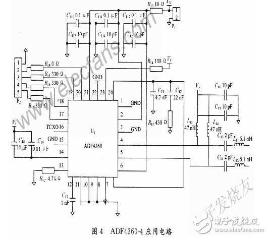
In the analog RF module, the ADF4360-4 provides the local oscillator signal for the mixer. The application circuit is shown in Figure 4. The frequency synthesizer receives an external temperature-compensated crystal oscillator, which is filtered and fed into the REFin pin (pin 16). The output pins (RFoutA and RFoutB, pins 4 and 5) deliver differential high-frequency signals to the mixer through a matching network and resonant filter. The CLK, DATA, and LE pins (pins 17–19) are connected to the MUXOUT pin (pin 20) for testing and interfacing with the FPGA. Pin 12 (Cc) is connected to ground through a capacitor, and pin 13 (Rset) sets the maximum current of the charge pump. Pin 14 (CN) is decoupled with a capacitor to Vvco. Separate power supplies for digital and analog circuits are used, with decoupling capacitors added for stability. The remaining analog and digital grounds are directly grounded.
The initial design of the frequency synthesizer involves setting up the configuration and ensuring proper signal integrity and stability. Proper placement of components, careful selection of reference oscillators, and accurate tuning of the loop filter are essential to achieving a clean and stable output signal.
Our company`s current transformers have high precision,wide range,small volume and good linearity that can be used to the field of electronic watt-hour meter, electric energy metering, electronic detection.
Performance
â—Power frequency insulation strength:The insulation between the primary winding and the secondary winding and the ground part of the CT can bear 4kV power frequency voltage for 1minute
â—Interturn insulation strength:The secondary open circuit, the primary winding through the rated current 1min, no inter-turn damage in the transformer
â—The deviation is better than the industry standards and national standards
Zero Phase Residual Ct,Small Type Current Transformer,Stable Current Transformer,Good Residual Current Transformer
Anyang Kayo Amorphous Technology Co.,Ltd. , https://www.kayoamotech.com