1 Introduction
CPLD is called complex programmable logic design chip, which is a large-scale programmable device with high integration, high reliability and high speed. CPLD is a carrier for electronic system design using EDA technology. The hardware description language is the main expression means of EDA technology for electronic system design. VHDL language is one of the commonly used hardware description languages. Software development tools are intelligent automatic design tools for electronic system design using EDA technology. Common development tools include Quartus II. , Ispexpert, FoundaTIon, etc. CPLD is widely used in electronic design due to its high speed, high reliability, and serial parallel operation. It breaks the boundaries between hardware and software and accelerates the product development process. The same single-chip microcomputer has the characteristics of high cost performance, flexible function, and good data processing capability. CPLD chips and single-chip microcomputers are widely used in high-performance instrumentation.
1 circuit simulation design
1.1 hardware circuit function
Using a MCS-51 chip, a CPLD/FPGA chip, an analog-to-digital converter ADC0809 and a digital-to-analog converter DAC0832 to form a data acquisition system, and use CPLD/FPGA to realize data sampling, D/A conversion output, and related data display. Control, the microcontroller completes the operation of A/D conversion data. The circuit is shown in Figure 1.
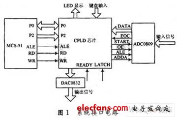
The system functions are as follows: The system collects the input voltage U1 at a certain rate, and converts it into 8-bit digital data through AD0809; the input data is input to the single-chip microcomputer after being sampled by CPLD/FPGA, and finally is sent to the DAC0832 through the CPLD/FPGA to be converted into ΔU. Data acquisition and processing are performed in an orderly manner under the management of the data acquisition system controller. The operating rate is determined by the rate of the clock signal CLK.
1.2 MCU and CPLD/FPGA interface design
The MCU uses the bus method to communicate data and control information with the programmable chip. This method has many advantages:
(1) Fast speed. Its communication working sequence is pure hardware behavior. For the MCS-51 microcontroller, only one single-byte instruction can complete the required read/write timings such as MOV@DPTR A and MOV A@DPTR.
(2) Save the I/O line of the CPLD chip. If the decoder in the figure is set with enough decoding output and enough latches are arranged, various types of data and control information can be exchanged between the FPGA/CPLD and the microcontroller through only 19 I/O lines. .
(3) Compared with the non-bus mode, the programming of the single-chip microcomputer is simple and reliable.
(4) It is easy to interface with SRAM or ROM by logic switching in FPGA/CPLD. In this way, high-speed data sampling is performed by FPGA/CPLD and high-speed A/D devices such as interfaces, and data is temporarily stored in SRAM. After the sampling is finished, the MCU and the SRAM are used to perform data communication in the bus mode by switching to take advantage of the powerful data processing capability of the MCU.
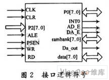
The system works as follows: ALE is the address latch enable signal. When the falling edge comes, the P0 port will send the lower 8 bits address to the address latch in the programmable chip CPLD/FPGA, and then in the P2 port and P0 port. The formed 16-bit address and the WR signal are combined to send the data of the P0 port to the programmable chip. The microcontroller writes data to the chip via two instructions, MOVXDPTR#ADDR and MOVX@DPTR A. Under the action of the 16-bit address formed by the P2 port and the P0 port and the RD signal, the AD0809 converted data is sent to the P0 port of the MCU. The MCU reads the data into the P0 port through two instructions MOVX DPTR#ADDR and MOVXA@DPTR. Set A/D conversion device chip select signal ad_e and DA conversion device chip select signal da_e, set data input/output port data[7. . 0]. The logic symbol generated by the MCU and FPGA communication interface program (named MCS51) is shown in Figure 2.
The CPLD uses the EPM7128 clock as a 16 MHz active crystal oscillator. First, the reset signal is sampled using CLK. The reset signal of the 8051 is required to be high for 2 machine cycles, 2 machine cycles are 2 & TImes; 12 = 24 oscillation cycles, reset. The signal is sampled continuously for 10 times. If it is always high, an on-chip reset enable signal is generated. Other on-chip registers are synchronously reset with this reset signal, and WR, RD, and ALE are sampled to avoid glitch interference.
1.3 AD0809 and CPLD/FPGA state machine interface design
1.3.1 AD0809 state machine function design
The simplest structure of the state machine is generally composed of two processes, namely, the master timing process and the master combination process. One process describes the sequential logic output, and the other process describes the combinational logic including the transfer logic of the interprocess status value and the output of the state transition value. The interface design system of AD0809 and CPLD/FPGA is divided into two parts, namely data unit and control unit. The data unit includes a data register that holds the operation data and the operation result, and a combinational logic circuit that performs the data operation. The control unit is used to generate a sequence of signals to determine when to perform data operations, and the control unit derives conditional signals from the data units to determine which data operations to continue. The data unit is to generate useful signals such as output signals and data operation states. There are two very important signals in the data unit and the control unit, namely the reset signal and the clock signal. The reset signal ensures the determinism of the initial state of the system, and the clock signal is a necessary condition for the operation of the timing system. The state machine usually returns to the initial state when the reset signal arrives, and the internal state changes when each clock arrives. Starting from the initial state of AD0809, that is, the state that started after the state machine is reset. Write a textual function description of this state when establishing each state. The function description of the AD0809 state machine and the corresponding pins are as follows:
S0 state: initial state, select the analog signal input of channel 1, ADDC='1', ALE=START=OE=LOCK='0';
S1 state: channel latched state. ALE='1',START=OE=LOCK='0':
S2 state: Start A/D conversion state. ALE='1', START='1', OE=LOCK='0';
S3 state: A/D conversion wait state, ALE=START='0', OE=LOCK='0';
IF EOC='0' keeps the current state unchanged, continues to wait for A/D conversion, ELSE conversion ends, and enters the next state;
S4 state: data output enable state, A/D conversion is completed, open data output enable signal, ALE='0', START'0', OE='1', LOCK='0';
S5 state: data latch state, open data latch signal, send conversion result to latch latch, ALE='0', START='0', OE='1', LOCK='0';
S6 state: delay state, in order to ensure reliable latching of data, delay one clock state period; ALE='0', START='0', OE='1', LOCK='1';
Other states: return to the initial state, ALE=START=OE=LOCK='0'.
1.3.2 ADC0809 State Machine Programming
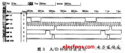
The ADC0809 is a unipolar input, 8-bit conversion precision successive-forward A/D converter. The sampling speed is about 100 μs per conversion. The address latch enable signal ALE locks the 3-bit address into the latch to determine the conversion signal path before the start of the conversion. EOC is the end signal of the conversion end. When the low level is turned to the high level, the end of the conversion is indicated. At this time, the converted 8-bit data can be read. EOC indicates that a conversion is in progress when it is low. START is the conversion start signal and the rising edge starts. OE is active high for data output. CLK is about 500 kHz for the ADC conversion clock input port. In order to achieve the highest conversion speed of the A/D device, the A/D converter controller must include logic to monitor the EOC signal. Once EOC is changed from low to high, OE is set high and then transmitted or displayed. Converted data [D0. . D7]. The state machine consists of three processes, ADC, AD_STATE, and DATA_LOCK. The ADC is the master combination logic process of this state machine. The system reset signal RST is first monitored during the output mode of the determination state and the output of the feedback control signal. When it is high, the process is reset to the initial state ST0. The start A/D conversion signal START turns on the output in state ST4 when the search transition state signal EOC changes from 0 to 1 in state ST3. The enable signal OE causes LOCK to generate an upper edge in the next state to initiate the process DATA_LOCK at this time to lock the 8-bit data converted by 0809 into the latch ADC_DATA. The connection to the CPLD/FPGA chip is completed by the state machine design program according to the timing circuit diagram. Figure 3 shows the simulation results of the state machine program.
Spiral Candle usually six colors , 22Gram Spiral Candle is the popular in Jeddah . every month we ship Spiral Taper Candle to Jeddah . we are about customer . so early receive deposit and ship fastly. Birthday Spiral Candles usually be used for party ,dinner ,festival . 22G Colorful Spiral Candle 's package details is each pcs WRAPPED BY CELLOPHANE,12PCS(2pc*6colors)IN ONE BLUE BOX AND box with SHRINK PACKED,24BOXES/CARTON. 22g Spiral Taper Candle can be loaded about 2200catons . we will try our best to load full .
Welcome to new and old customer order !
22Gram Spiral Candle,22G Colorful Spiral Candle,Birthday Spiral Candles,Spiral Taper Candle
Shijiazhuang Zhongya Candle Co,. Ltd. , https://www.zycandlefactory.com