Nexys3 Learning Notes 3: Hardware peripherals

Get a new board, usually we can't wait to run a test demo to see the effect, but please believe that this is a "novice" feature. We are no longer young, and there is no need to "recklessly" toss the board. Returning to rationality, then I suggest that you may wish to take a look at the schematic diagram first, then compare the board with the actual object, simply digest the whole circuit, and figure out the specific usage and precautions of the onboard jumper, power socket, etc., so as not to stage the "high voltage." The tragedy of smoking.

The schematic of the Nexys3 is available on the official website of Digilent (download address:). For schematics, you usually need a certain amount of hardware skills to be able to easily see. Of course, the general development board will be equipped with a more detailed circuit description (this development board can be referenced), it is recommended that you may wish to look at it first, and then digest the schematic.

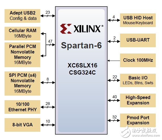
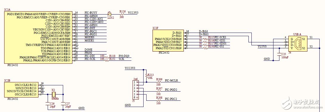
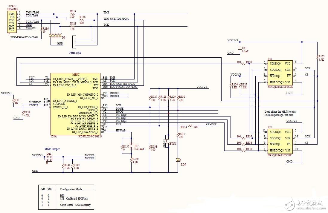
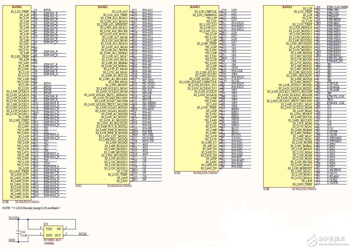
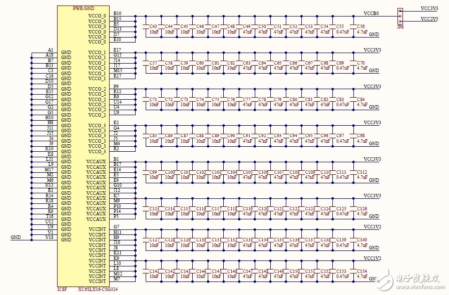
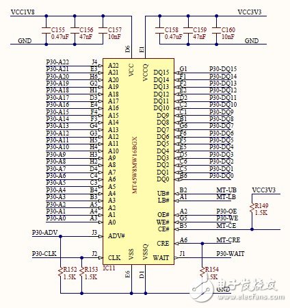
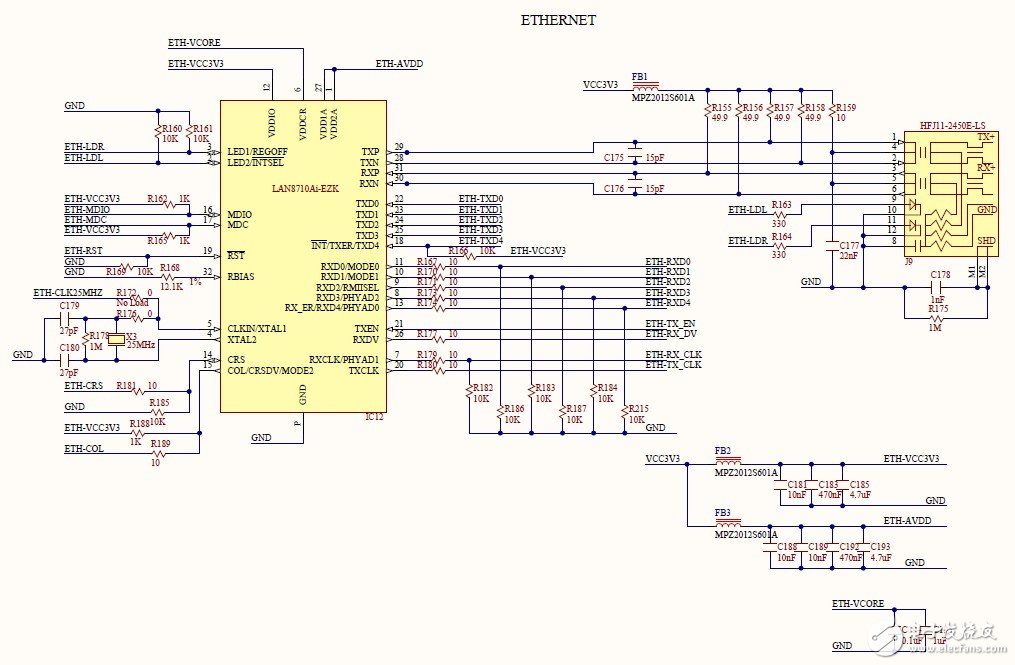
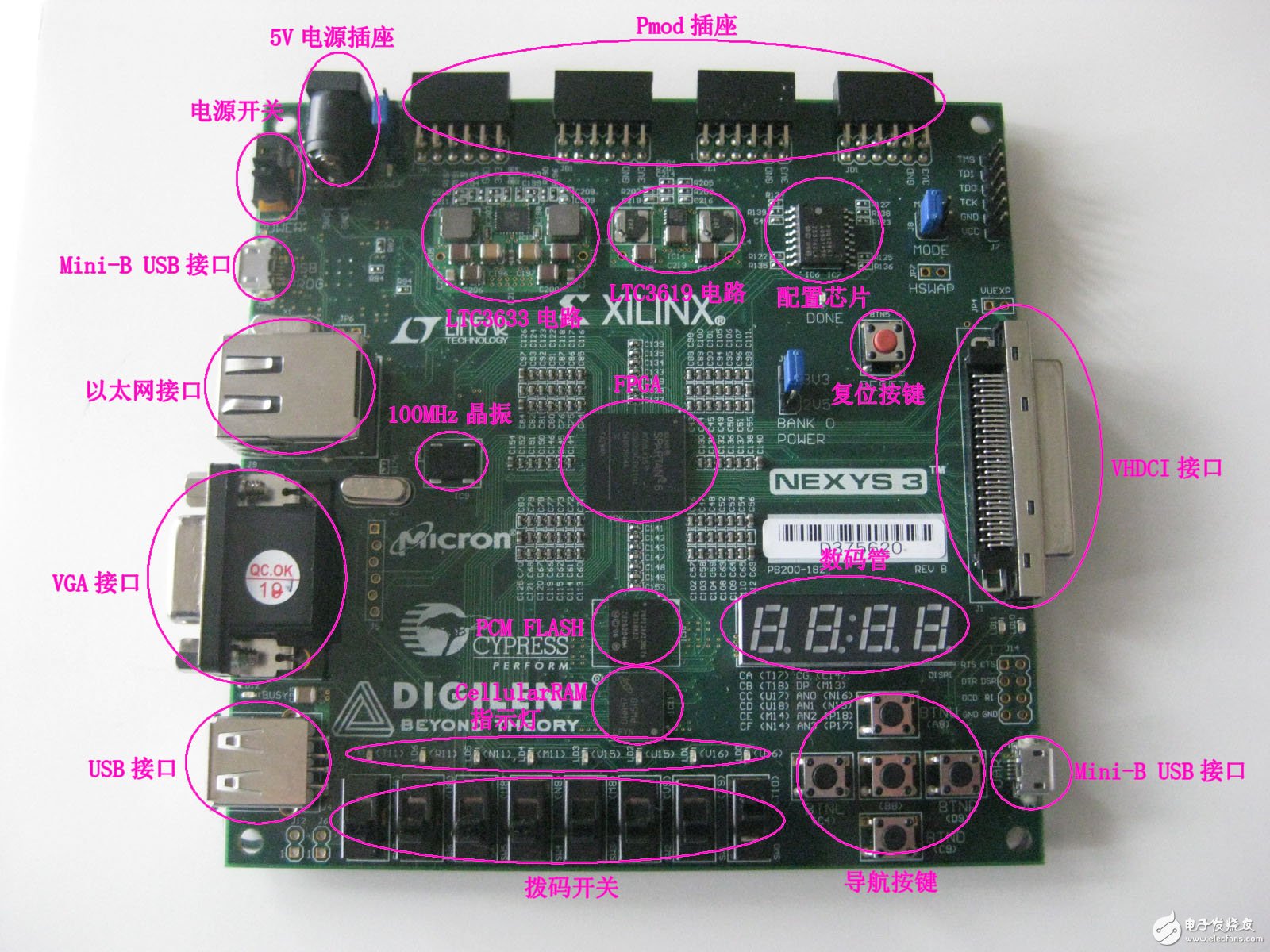
The overall hardware architecture of the Nexys3 board is illustrated in Nexys3_rm.pdf (reference manual), as shown in Figure 1. The XC6SLX16 device around the main chip Spartan-6 has a wealth of onboard peripherals such as Cellular RAM, parallel PCM nonvolatile memory, SPI interface PCM nonvolatile memory, 10/100 Ethernet physical layer interface, 8-bit VGA interface, USB HID host, USB-UART bridge chip and some basic IO peripherals (indicators, buttons, switches, etc.), in addition to FPGA USB download configuration circuit, 100MHz working clock and other expansion interface sockets.

Nexys3 Learning Notes 3: Hardware peripherals

Figure 1 Nexys3 overall circuit block diagram
The schematic of Nexys3 is 10 pages in total, and we interpret them one by one.

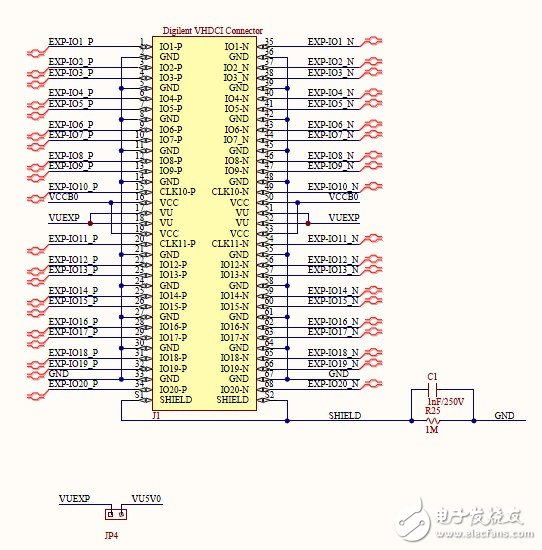
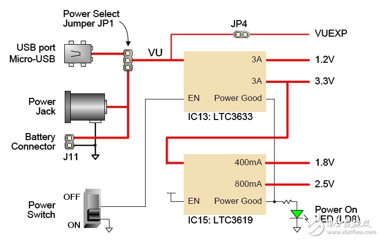
J1 in Page1 is a high-speed VHDCI socket interface, as shown in Figure 2. It is not difficult to conclude from the schematic diagram and signal naming of the schematic that the signals directly derived from the FPGA should be high-speed serial differential pairs. In addition, we need to note that JP4 can be used to short-circuit the power supply VUEXP introduced by J1 and the on-board power supply VU5V0. In other words, if the 5V power supply introduced by J1 is used, JP4 can be shorted.

Nexys3 Learning Notes 3: Hardware peripherals

Figure 2 High-speed VHDCI interface
Another part of the circuit of Page 1 is shown in Figure 3. Here, four sets of 8-bit signal Pmod sockets are introduced. Each data signal passes through a 200 ohm matching resistor and has a grounded protection diode. For the general expansion, the four sets of data lines and the corresponding power and ground are basically more than enough.

Nexys3 Learning Notes 3: Hardware peripherals

Figure 3 four groups of Pmod interfaces
In Page 2, it is basically a simple common interface circuit. Figure 4 is a 4-way independent button circuit. When the button is not pressed, it is equivalent to the IO pin of the FPGA connected to the 20K resistor and pulled down to the ground. When the button is pressed, it is equivalent to pulling up 10K to the voltage VCCB0. Figure 5 is an 8-way independent DIP switch circuit. The IO pin of the FPGA is connected to GND or VCC3V3 through a 10K resistor. Figure 6 is a 4-segment digital tube circuit with a common anode at the common end and a triode control switch connected via an IO pin. Figure 7 is an 8-bit color VGA interface circuit. The output voltage of the IO pin is divided by resistors to obtain up to 256 color combinations. Figure 8 is a common 8-bit indicator circuit.

Nexys3 Learning Notes 3: Hardware peripherals

Figure 4 button circuit

Nexys3 Learning Notes 3: Hardware peripherals

Figure 5 DIP switch circuit

Nexys3 Learning Notes 3: Hardware peripherals

Figure 6 digital tube circuit

Nexys3 Learning Notes 3: Hardware peripherals

Figure 7 VGA interface

Nexys3 Learning Notes 3: Hardware peripherals

Figure 8 indicator circuit
Page 3 is mainly the circuit of high-speed USB microcontroller chip CY7C68013A, which is divided into 5 parts in the schematic diagram. Figure 9 shows the interface signal between CY7C68013A and FPGA; Figure 10 includes the crystal input, each control signal and the signal of the USB port; Figure 11 shows the circuit of the power supply and part of the decoupling capacitor. Figure 12 is a 5PIN Mini-B type USB interface socket connection circuit. Figure 13 is a circuit of an EEPROM chip connected to the CY7C68013A, which can be used as the ROM of the 8051 microcontroller in the CY7C68013A chip.

Nexys3 Learning Notes 3: Hardware peripherals

Figure 9 CY7C68013A circuit 1

Nexys3 Learning Notes 3: Hardware peripherals

Figure 10 CY7C68013A circuit 2

Nexys3 Learning Notes 3: Hardware peripherals

Figure 11 CY7C68013A circuit 3

Nexys3 Learning Notes 3: Hardware peripherals

Figure 12 Mini-B type USB socket circuit

Nexys3 Learning Notes 3: Hardware peripherals

Figure 13 EEPROM chip circuit
There is a 16-bit MCU in Page 4, PIC24 has a wealth of peripherals, including the USB interface in Figure 14, which can be used as the host control of the current mainstream USB mouse and keyboard. The PIC24 part of the signal pin is connected to the FPGA and uses an 8MHz external crystal.

Nexys3 Learning Notes 3: Hardware peripherals

Figure 14 PIC interface circuit 1
As shown in Figure 15, the J6/J12 can lead to the analog pins of the PIC24. It can be seen that the PIC24 integrates the peripheral functions of the AD/DA. Figure 15 also illustrates the power supply to the PIC24 and the corresponding decoupling circuitry.

Nexys3 Learning Notes 3: Hardware peripherals

Figure 15 PIC interface circuit 2

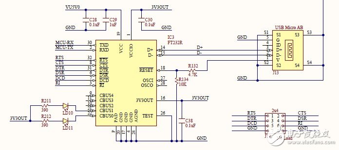
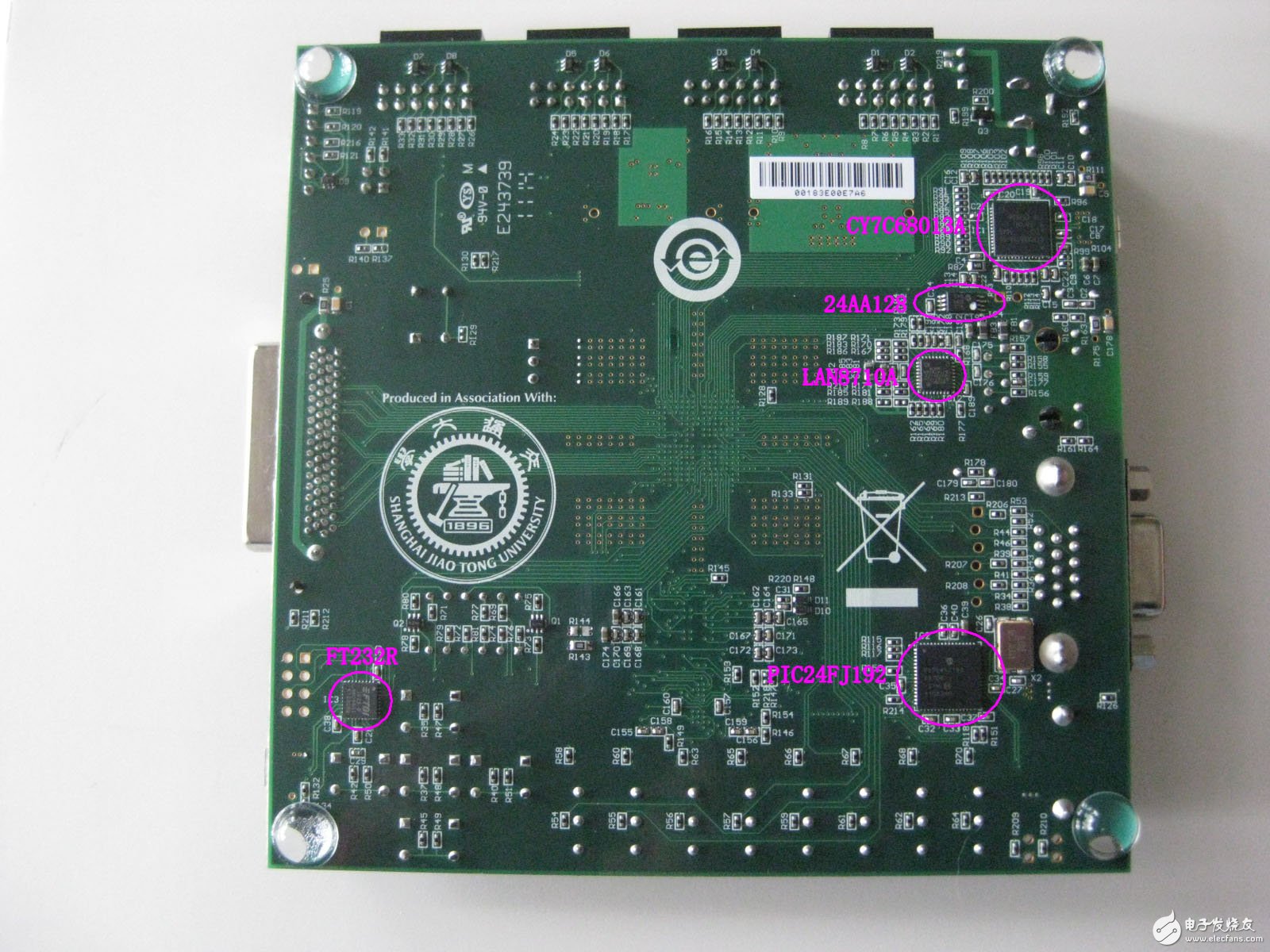
As shown in Figure 16, the FPGA is also connected to a RS232-USB bridge chip FT232. The chip provides a standard set of RS232 interfaces (J14 also provides additional extensions for these interfaces) to connect to the FPGA, and the other end can communicate as a USB protocol interface.

Nexys3 Learning Notes 3: Hardware peripherals

Figure 16 FT232 circuit
Page 5, as shown in Figure 17, is mainly the configuration circuit of the FPGA, including the FPGA part configuration schematic part (IC8A), two pieces (the actual PCB is made of double or single) to store the PROM chip (IC6/IC7) ), download the configuration socket (J7). There is also a two-digit jumper socket J8, and the schematic diagram also shows that different jumper modes can implement BPI, SPI and Slave Serial configuration.

Nexys3 Learning Notes 3: Hardware peripherals

Figure 17 FPGA configuration circuit
Page 6 is mainly the definition of the IO pin signal of the FPGA and the 100MHz clock crystal oscillator circuit of the external input of the FPGA, as shown in Figure 18.

Nexys3 Learning Notes 3: Hardware peripherals

Figure 18 FPGA IO pin definition
Page 7 is the power supply circuit of the FPGA. As shown in Figure 19, basically every VCC pin has a corresponding high and low decoupling capacitor. It should be noted that the jumper cap JP8 can be powered by VCV_0 with 2.5V or 3.3V. The IO power of this bank is reserved for some special level applications.

Nexys3 Learning Notes 3: Hardware peripherals

Figure 19 FPGA power circuit
In Page 8, two pieces of Micron's PCM memory, which is very fashionable at the moment. As shown in Figure 19, it is a piece of CellularRAM chip. This kind of RAM is not used in the past RAM. It combines the advantages of RAM and DRAM, and can be accessed at high speed and easily and quickly. As shown in FIG. 20, it is a parallel PCM FLASH chip.

Nexys3 Learning Notes 3: Hardware peripherals

Figure 20 Memory Interface 1

Nexys3 Learning Notes 3: Hardware peripherals

Figure 21 Memory Interface 2
Page 9, as shown in Figure 22, is an Ethernet circuit that includes an Ethernet transceiver chip LAN8710 and a corresponding crystal head socket.

Nexys3 Learning Notes 3: Hardware peripherals

Figure 22 Ethernet circuit
Page 10 is the entire supply voltage generation circuit of the system. Two Linear DC/DC chips were used, as shown in Figures 23 and 24. The interface between the entire system chip is basically 3.3V, the core voltage of the FPGA is 1.2V, and the PCM FLASH uses 1.8V. The 2.5V is mainly reserved. The introduction of the power supply also uses two methods, which can be switched by the jumper cap JP1, that is, the common jack socket or USB power supply.

Nexys3 Learning Notes 3: Hardware peripherals

Figure 23 power circuit 1

Nexys3 Learning Notes 3: Hardware peripherals

Figure 24 power circuit 2
In the reference manual, there is a schematic diagram of the power supply shown in Figure 25.

Nexys3 Learning Notes 3: Hardware peripherals

Figure 25 Power supply schematic
The whole schematic diagram is digested, and you may encounter some chips that you have never met before. It doesn't matter. Put these chips together and go to their official website. The download datasheet has a general view and it will be digested. The main chips involved in Nexys3 are shown in Listing 1. Table 1 Nexys3 main chip list Chip type website CY7C68013A-56USB(MCU)#PBFPOWER#PBFPOWER

Anatomy of the board

Seeing more of the schematics, it is inevitable that aesthetic fatigue. Let's take a break. The privileged classmates will not talk nonsense. According to the previous schematic diagram, as shown in Figure 26 and Figure 27, the main chip and connectors are taken out one by one.

Nexys3 Learning Notes 3: Hardware peripherals

Figure 26 shows the front of the board

Nexys3 Learning Notes 3: Hardware peripherals

Figure 27 The back of the board is reprinted from: The blog of the privileged classmate

PV Cable

The cables are for the solar system.

Solar Cable,Pv Wire,Solar Dc Cable,Dc Wire For Solar Panels

NANTONG RONGCHANG IMPORT&EXPORT CO.,LTD , https://www.ergsolarcn.com