AMOLED (AcTIve Matrix/Organic Light EmitTIng Diode) is an active matrix organic light emitting diode panel. Compared with traditional liquid crystal panels, AMOLED has the characteristics of faster response, higher contrast, and wider viewing angle.
Because AMOLED has inherent advantages over TFT LCD in terms of image quality, performance and cost. This is why many international companies still do not give up developing AMOLEDs despite their difficult yield. At present, we continue to invest in the development of AMOLED manufacturers, in addition to Sony, which has already announced the time to market, Toshiba, which invests in Toshiba Matsushita Display (TMD), and Panasonic, which has separately developed products, and Sharp, which claims to be not optimistic. The NOKIA N85 released in August 2008 and the NOKIA N86 launched in the first quarter of 2009 all use AMOLED.
In terms of display performance, AMOLED has faster response speed, higher contrast ratio and wider viewing angle. These are places where AMOLED is better than TFT LCD. In addition, AMOLED has self-illuminating features, no need to use backlight, so it is more than TFT. It can be made thinner and more power efficient. There is also a more important feature. AMOLED without backlighting can save the cost of backlight module which accounts for 3~4% of TFT LCD.
AMOLED is indeed a very attractive product. Many international manufacturers like it. Even the iPhone, the most popular product in the mobile phone market, is interested in AMOLED. I believe that after the yield increase, the iPhone will also consider adopting AMOLED, especially AMOLED. The characteristics of power saving are very suitable for mobile phones. At present, the power consumption of AMOLED panels is only about 60% of TFT LCD, and there is room for further decline in future technologies.
Of course, the biggest problem with AMOLED is the yield. At the current yield, the price of AMOLED panels is 50% higher than that of TFT LCD. This is a threshold for customers to use a lot, but for Qijing, now The stage is also in the training period of the adjustment rate, and it is not easy to take orders in large quantities.
(1) Metal oxide TFT
This production technology is currently favored by many manufacturers and professional survey companies, and is considered to be the first choice for large-size AMOLED technology routes in the future. Each company also has corresponding large-size samples on display.
The TFT substrate of the technology can adopt a mature and large-scale sputtering film formation method in the liquid crystal industry, and the oxide is InGaO3 (ZNO) 5, although the electron mobility of the device is higher than that of the LTPS technology. The product is low, basically 10 cm2/V-sec, but this mobility parameter is more than 10 times that of the amorphous silicon technology device. The electron mobility of the device can fully meet the current driving requirements of AMOLED, so it can be applied to OLED. Drive.
At present, metal oxide technology is still in the laboratory verification stage. There is no real experience of overproduction in the world. The main factor is that its reproducibility and long-term work stability need further improvement and confirmation.
(2) Low temperature polysilicon technology (LTPS TFT)
This technology is currently the only AMOLED production technology in the world that has been commercialized and mass-produced and proven to be quite mature in the production line below G4.5.
The main difference between this technology and amorphous silicon technology is the use of laser crystallization to convert amorphous silicon film into polysilicon, thereby increasing the electron mobility from 0.5 to 50-100 cm2/Vs to meet the requirements of OLED current drive. .
After years of commercial mass production, the technology has superior performance and good work stability. At the same time, in the mass production of these years, the yield rate has been greatly improved, reaching about 90%, greatly reducing the product. cost.
It can be seen from the above LTPS process flow that the main difference between it and the amorphous silicon technology is that the laser crystallization process and the ion implantation process are added, the other processing processes are basically the same, and the equipment has similarities with the amorphous silicon production.
In addition, there are many kinds of crystallization technology. At present, ELA is the most commonly used small size. Other crystallization technologies include: SLS, YLA, etc. Some companies are also using other technologies to develop TFT substrates for AMOLEDs, such as metal induction. Crystallization technology, there are corresponding samples on display, but the main problem of this technology is that metal will lead to voltage breakdown between layers, leakage current is large, device stability can not be guaranteed (because AMOLED devices are particularly thin, each layer It is an important issue to ensure the cleanliness of the layer during processing and prevent voltage breakdown.
The main defects of LTPS technology are as follows:
â— The production process is more complicated, and the number of Masks used is 6-9, and the initial equipment input cost is high.
â— Due to the limitation of laser crystallization process, large size is difficult. The largest production line is G4.5.
â— Laser crystallization causes Mura to be severe, and it is used on TV panels, which causes visual defects.
(3) Amorphous silicon technology (a-Si TFT)
The most successful application of amorphous silicon technology is in the liquid crystal production process. Currently, most LCD manufacturers use a-Si technology except for a few LTPS technologies.
The a-Si technology has high maturity in the liquid crystal field, and its device structure is simple. Generally, it is 1T1C (1 TFT thin film transistor circuit, 1 storage capacitor), and the number of Masks used in manufacturing is 4-5. At present, there are also manufacturers studying. 3Mask process.
In addition, the a-Si technology is used for the production of AMOLED, and the equipment can completely use the original equipment processed by the current liquid crystal TFT, and the initial input cost is low.
Furthermore, the large-scale realization of amorphous silicon technology has been fully realized, and currently it has achieved more than 100 inches in the field of LCD.
Although a-Si technology is the mainstream in the LCD field, OLED devices are current-driven, and the low electron mobility of a-Si devices cannot meet this requirement, although some companies (such as IGNIS in Canada) design ICs. Some improvements have been made, but it is still not possible to solve the problem fundamentally.
The main technical bottleneck of LTPS technology is the crystallization process, while the a-Si technology has no technical problems in the manufacturing process, but the design of the matching IC is very high, and the current IC manufacturers are mainly LTPS, a-Si The investment in IC development is small, so if a-Si technology is used for production, the source of IC is a serious bottleneck and a constraint, and the performance of the device will be greatly reduced.
(4) Microcrystalline Silicon TFT
The microcrystalline silicon technology is basically the same as the amorphous silicon technology commonly used in LCDs in material use and film structure.
The micro-silicon technology device has an electron mobility of 1 to 10 cm2/Vs, which is currently selected by Sony.
Although this technology can also achieve the purpose of driving OLEDs, due to its low electron mobility and poor display performance, there are few manufacturers selected as research directions.
Through comparison of various TFT technologies, we can see that the main advantage of LTPS technology is that the electron mobility is extremely high, fully meeting the driving requirements of OLED, and after several years of commercial production, the yield rate has reached about 90%, production. High maturity. The main problem is that the initial equipment input cost is high and the large size is difficult.
Metal oxide technology Although the electron mobility is not as high as LTPS, it can meet the driving requirements of OLEDs, and its large size is relatively easy. The main problem is poor stability and no mature production processes.
Although the microcrystalline silicon and amorphous silicon technologies are relatively simple and easy to realize large size, and can be manufactured on the current LCD production line, the initial input cost is low, but the main problem is low electron mobility, suitable for LCD. Voltage driven, not suitable for OLED current drive mode, and there is no mature production experience in OLED, device stability and process maturity cannot be guaranteed.
Combining the actual situation of all AMOLED manufacturers in the world and the comparison and analysis of several technologies above, we believe that Guangdong Province should adopt low temperature polysilicon technology (LTPS) technology and adopt laser crystallization method in TFT substrate technology. . At the same time, the development of metal-induced methods is encouraged. If a breakthrough can be made in metal induction, it can also be used as a technical direction.
(5), organic film evaporation technology route selection
The organic layer formation method can be divided into a traditional method and a novel method. The traditional approach is based on vapor deposition technology, and the emerging approach is based on transfer and printing technologies.
In the emerging mode, transfer technology was jointly developed and developed by Samsung and 3M; printing technology was mainly developed and developed by Epson. The biggest advantage of these two methods is to improve the material utilization rate and simplify the production process, but its technology and materials have a certain monopoly, and currently do not have the ability to mass production.
The traditional vapor deposition method is also the CVD we usually talk about. For the evaporation of organic materials, it is divided into point source type, line source type and OVPD (organic vapor deposition) according to the difference of evaporation source and evaporation mode.
Developed by Axon, Germany, OVPD has improved processability and reduced manufacturing costs compared to evaporation technology. Excellent repeatability and process stability, as well as significant film uniformity and precise control of doping, lay the foundation for high-yield mass production while reducing maintenance and cleaning requirements, thereby reducing material consumption and improving materials Great potential for utilization.
The OVPD method has better superiority and is developed by non-OLED manufacturers. It is a relatively promising production technology and equipment for the vast number of OLED manufacturers. But the device currently has two problems:
1) The current mature equipment can only be made to the size of 370 & TImes; 470, and can not meet the requirements of large-scale production.
2) The device currently has good reliability for monochrome devices, but the stability of full color is not ideal.
In view of the above analysis, we can only use the evaporation method of point source or line source. At present, the point source technology Japan TOKKI company is relatively excellent, and the line source technology Japan ULVAC company is relatively excellent. Hongwei can also work hard in this regard.
(6), light injection mode technical route selection
At present, OLED devices have two modes of light emission: bottom emission and top emission. The following table compares the two methods:
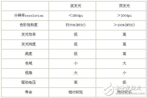
The bottom illuminating technology is mature, and the risk of selection is small, even without risk. There are two difficulties in the top illuminating process: one is cathode fabrication and the other is packaging. Despite the difficulty of the top luminescence, it is already the trend (at least there is no new breakthrough in the backsheet material). However, in the long run, if the backboard material has a new breakthrough, such as the improvement of the mobility and uniformity, then the bottom light has the advantage of lower cost. In general, with the a-Si backplane, top illumination is a better choice; the P-Si backplane can consider the bottom illumination.
Material: Malleable Iron
Type: Double bolts Hose Clamps, Interlock hose clamps, other special type
Double bolts hose clamps size: SL-22,SL-29,SL-34,SL-40,SL-49,SL-60,SL-76,SL-94,SL-115,SL-145,SL-400,SL-463,SL-525,SL-550,SL-600,SL-675,SL-769,SL-818,SL-875,SL-988,SL-1125,SL-1275, SL-1450
Interlock clamps size: 1/2" to 2"
Application: Pipelines,brackets

Material: ASTM A197
Finishing: Hot dipped galvanized
Application: Connection with pipes for Industry, Market or Home.
Size:
| Pipe Clamp Size | Normal Size inch | O.D. in mm |
| T21 | 1/2" | 21.3 |
| A27 | 3/4" | 26.9 |
| B34 | 1" | 33.7 |
| C42 | 1-1/4" | 42.4 |
| D48 | 1-1/2" | 48.3 |
| E60 | 2" | 60.3 |

Pipe Clamps,Tube Clamp,Pvc Pipe Clamps,Conduit Clamps
HEBEI ZIFENG NEW ENERGY TECHNOLOGY CO.,LTD. , https://www.zifengpipeline.com