0 Introduction High-resolution visible light camera is one of the most important means of space remote sensing, and it has broad application prospects in both commercial and scientific research fields. The development of high-resolution visible light cameras has become an important indicator of a country's scientific and technological level. At present, users' requirements for ground resolution are constantly improving. The development of high-resolution optical remote sensors has become a hotspot in the field of space remote sensing in the world. High-resolution visible light cameras have been developed abroad earlier, and developed countries such as the United States have developed high-resolution visible light cameras. The development of high-resolution CCD cameras in China started late, and there is still a certain distance from the level of developed countries. There are many factors that affect the resolution of the camera. Low-noise video processing technology is one of the keys to achieving high-resolution imaging capabilities of the camera.
This article refers to the address: http://
1 CCD device noise and noise processing
The noise of CCD devices mainly includes photon noise, shot noise, fat zero noise, transfer noise, dark current noise and output noise [1]. Noise is the main factor affecting the CCD output image signal.
In the CCD application, the following measures have been taken to suppress and eliminate the above noise [3]:
(1) In the circuit process, increase the filtering of the DC power supply to eliminate interference from the power supply. Shorten the connection between the driver circuit and the CCD device, and reduce the spike interference caused by the clock induction. The digital ground is separated from the analog ground to reduce interference from the ground.
(2) For the transfer noise, the CCD voltage is reversed or the substrate voltage is increased to reverse the CCD voltage, which can eliminate the interface state trapping noise; lowering the operating temperature can significantly reduce the trapping noise.
(3) For shot noise, an adjacent pixel (or adjacent line) integral averaging method is used to remove or adjacent multi-frame averaging. (4) Dark current noise: For a CCD with a darker average current of each pixel, if there are a small number of dark pixels at the beginning of the pixel array, the output signal is sampled and stored, and with the subsequent valid pixels. The output signal samples are subtracted to remove dark current noise. However, it must be ensured that the integration time and temperature of the two samples are the same.
(5) A low-pass filter with a cutoff frequency of 2f (f is the CCD readout frequency) can be used for the output noise. There are also related double sampling method (CDS), double oblique integration method (DSI), clamp removal method (CCS) and so on.
2 TDICCD video signal processing video processing circuit is mainly to remove the reset pulse interference and noise signal, consisting of preamplifier, correlated double sampling, clamp, filter output, line buffer, output interface circuit and other links. The CCD video processing circuit is shown in Figure 2-1.
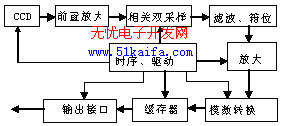
Figure 2-1 Block diagram of the video processing circuit
The image signal received by the CCD image sensor is preamplified and becomes a differential signal output. After the differential receiving circuit, it is converted into a single-ended video signal, and subjected to correlated double sampling processing by CDS to obtain a "clean" video signal, and then subjected to low-pass filtering. The filter filters out the spike interference of the CCD driving pulse, and is amplified by the controllable gain amplifying circuit to the level required by the A/D converter, and is subjected to A/D conversion to become a digital image signal, which is alternately buffered by a buffer (FIFO). The LVDS interface chip is driven and output.
In the actual design, Philips' special CCD camera interface chip TDA8783 is used to realize.
2.1 Introduction to TDA8783
TDA8783 is a 10-bit analog-to-digital interface chip dedicated to CCD camera by PHILIPS. It is mainly composed of correlated double sampling circuit (CDS), gain control circuit (AGC), clamp circuit, low power 10bit analog-to-digital converter (ADC). ) Composition [5]. The functions of the system can be completed by implementing on-chip three-wire serial port programming to achieve on-chip DACs allocation.
2.2 preamplifier circuit
The signal level of the CCD output decreases as the accumulated charge increases. Amplification and differential output are required for long-distance transmission and reduced common mode interference introduced during transmission. The preamplification is to amplify the output signal of the CCD to a sufficient amplitude.
In this system, the AC coupling is adopted between the preamplifier and the CCD output terminal, which eliminates the DC level, which is beneficial to the matching between the two stages, and also eliminates the influence of the zero drift caused by temperature and other factors on the transmission signal. Of course, the use of AC coupling causes loss of DC components in the signal, which can be recovered by subsequent clamp circuits.
2.3 Related Double Sampling (CDS)
To ensure that a high signal-to-noise ratio video signal is output, the noise must be processed. The correlated double sampling (CDS) technology not only can filter the reset noise well, but also has certain filtering for the horizontal clock drive of the TDICCD sensor and the ground-line coupled crosstalk noise of the power supply, the white noise of the output amplifier, and the 1/f noise. In addition to the role [4].
In this system, we use CCD camera interface chip TDA8783 to realize CCD video signal processing. It contains a correlated double sampling (CDS) module, which can effectively process the CCD output signal and eliminate the KTC noise of CCD. The CDS programmable bandwidth is 4 to 120 MHz; the input peak voltage is 400 mV; and the output amplifier gain is 6 dB. In use, the internal control DAC can be selected by programming the external three-wire serial port to implement the CDS function. When the serial port shift register address A2A1A0 = "001", the on-chip 4bit DAC works to control the CDS operation. The sampling rate in this system is 4MHz, and the 4-bit DAC input code is set to D3D2D1D0=“0001â€.
2.4 Gain Control In order to adapt to different brightness targets and prevent signals from being too weak or saturated, a gain selection amplifier circuit should be designed in the video signal processing circuit. According to the brightness of the ground target, select the corresponding gain. The CCD camera interface chip TDA8783 integrates a gain controller (AGC) with a minimum gain of 4.5dB and a maximum gain of 34.5dB. The internal logic of the gain control of the TDA8783 is shown in Figure 2-2. The gain control function is realized by programming the three-wire serial port. When the serial port input shift register address A2A1A0=“010â€, the 9 bit control DAC works; when the input code is “00â€, the minimum gain is 4.5dB, and the input code is greater than When it is equal to "319", the output gain is 34.5dB. 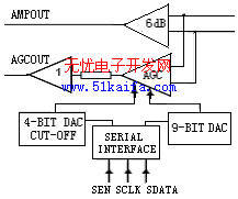
Figure 2-2 Internal logic diagram of gain control
2.5 Clamp and filter circuit
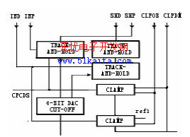
Figure 2-3 Input clamp internal logic block diagram
The signals output by the correlated double-sampling processing circuit are mixed with sampling spikes and other high-frequency interference signals. This requires low-pass filtering circuits to filter out high-frequency interference and select useful video signals with lower frequencies. At the same time, the preamplifier adopts AC coupling, and the negative AC signal is correlated with double sampling to remove noise, and appears in the positive polarity form at the output of the correlated double sampling circuit. Unnecessary negative polarity components are introduced during the two sampling and subtraction processes. Since the A/D conversion circuit requires that the input analog quantity cannot be negative, a clamp circuit is provided to remove the negative level in the low pass filtered signal.
The TDA8783 includes a bandwidth control circuit and a clamp control circuit that enables bandwidth control and clamp control by programming the on-chip three-wire serial port. The internal logic of the TDA8783's clamp control is shown in Figure 2-3. When the serial port input shift register address A2A1A0=“001â€, the on-chip 8 bit DAC works to control the bandwidth. At this time, D3~D0 are used to set the CDS bandwidth, D4~D7 are used to set the AGC bandwidth; when the serial port inputs the shift register address When A2A1A0 = "100", the on-chip 10-bit DAC operates to control the input clamp level of the ADC (analog-to-digital converter).
When the input code is "0", VDACOUT (ADC clamp control DAC output voltage) is 1.5V; when the input code is "1023", VDACOUT is 2.5V.
2.6 The output of the analog-to-digital conversion video processing circuit is an analog signal. In order to facilitate data compression and transmission, it needs to be converted into a digital signal. The analog-to-digital conversion circuit [2] converts the analog video signal into a digital video signal under the control of the timing pulse. And drive the output in the specified format. According to the technical requirements, the radiation quantization level is 8bit, and it is necessary to use the A/D chip output with a sampling rate greater than 10MHz. In order to obtain a high quality quantized signal, it is necessary to carefully select an A/D converter with a high performance parameter.
In this system, the TDA8783 integrates a 10bit A/D converter. The maximum sampling frequency of the ADC (analog-to-digital converter) can reach 40MHz, the minimum clock pulse width is 12ns, the duty ratio is 1:1, the input peak voltage is 2V, the maximum input current is 120, and the +5V single-supply power supply, the typical nonlinear error is 0.2LSB. The maximum sampling delay is 5 ns.
When performing A/D conversion, it is necessary to correctly determine the sampling point of the A/D conversion, that is, the position of the sampling pulse on the analog signal (the sampling point must be placed on the effective and stable analog signal segment), otherwise it may be The sampling point falls in an unstable position of the signal, and an error signal is generated, or the sampling point falls outside the signal to generate an error signal.
2.7 Data output interface The data output adopts LVDS differential output. The output signals of each channel are: one pixel clock, one line sync signal and digital image signal. The image data, line sync, and pixel clock signals are driven by the interface circuit and output. The interface chip uses the DS90C031 of NS.
3 Conclusions (1) Only the correct design of the system's timing drive signal can complete the coordination of the entire circuit;
(2) The preamplifier circuit of the CCD output video signal should also be as close as possible to the sensor, CCD video signal processing circuit
Should also be as close as possible to reduce the noise interference introduced during transmission;
(3) After the CCD signal is processed by the video processing circuit, the signal quality is greatly improved to meet the requirements of the system index.
CCTV Camera,Consumer Electronics,Video Camera & Accessories,Hunting Camera
Camera Co., Ltd , http://www.nbcamera.com